gf180mcu_fd_sc_mcu7t5v0__xor2_4
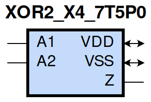
gf180mcu_fd_sc_mcu7t5v0__xor2_4 symbol
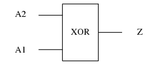
gf180mcu_fd_sc_mcu7t5v0__xor2_4 schematic

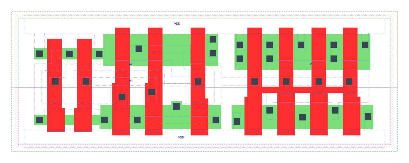
gf180mcu_fd_sc_mcu7t5v0__xor2_4 layout
XOR2_X4 is a 2-input exclusive OR, 4X drive strength
Attribute |
Value |
area |
48.294400 µm2 |
Output Pin |
Function |
Z |
(A1^A2) |
A1 |
A2 |
Z |
1 |
0 |
1 |
0 |
1 |
1 |
1 |
1 |
0 |
0 |
0 |
0 |
Pin |
Type |
Capacitance (pf) |
A2 |
input |
0.0072 |
A1 |
input |
0.0069 |
Input Pin |
Output |
When Condition |
Tin (ns) |
Out Load (pf) |
Delay (ns) |
Tout (ns) |
A2(HL) |
Z(HL) |
!A1 |
0.0100 |
0.0010 |
0.4620 |
0.0716 |
A2(LH) |
Z(LH) |
!A1 |
0.0100 |
0.0010 |
0.3166 |
0.0487 |
A2(HL) |
Z(LH) |
A1 |
0.0100 |
0.0010 |
0.5309 |
0.0473 |
A2(LH) |
Z(HL) |
A1 |
0.0100 |
0.0010 |
0.4790 |
0.0533 |
A1(LH) |
Z(HL) |
A2 |
0.0100 |
0.0010 |
0.4915 |
0.0533 |
A1(HL) |
Z(LH) |
A2 |
0.0100 |
0.0010 |
0.5835 |
0.0496 |
A1(LH) |
Z(LH) |
!A2 |
0.0100 |
0.0010 |
0.2845 |
0.0467 |
A1(HL) |
Z(HL) |
!A2 |
0.0100 |
0.0010 |
0.4310 |
0.0714 |
Input Pin |
When Condition |
Tin (ns) |
Output |
Out Load (pf) |
Energy (uW/MHz) |
A2 |
!A1 |
0.0100 |
Z(HL) |
0.0010 |
1.0327 |
A2 |
A1 |
0.0100 |
Z(HL) |
0.0010 |
0.8639 |
A1 |
A2 |
0.0100 |
Z(HL) |
0.0010 |
0.8872 |
A1 |
!A2 |
0.0100 |
Z(HL) |
0.0010 |
1.0047 |
A2 |
!A1 |
0.0100 |
Z(LH) |
0.0010 |
0.5960 |
A2 |
A1 |
0.0100 |
Z(LH) |
0.0010 |
0.7672 |
A1 |
A2 |
0.0100 |
Z(LH) |
0.0010 |
0.8320 |
A1 |
!A2 |
0.0100 |
Z(LH) |
0.0010 |
0.5370 |
When Condition |
Power (nW) |
!A1&!A2 |
0.2325 |
A1&A2 |
0.3184 |
!A1&A2 |
0.3081 |
A1&!A2 |
0.2322 |