gf180mcu_fd_sc_mcu7t5v0__and2_2
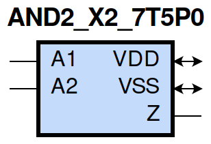
gf180mcu_fd_sc_mcu7t5v0__and2_2 symbol
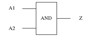
gf180mcu_fd_sc_mcu7t5v0__and2_2 schematic

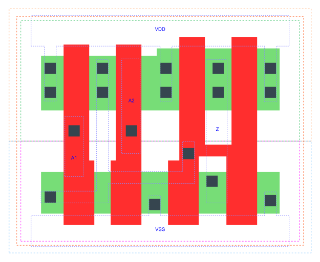
gf180mcu_fd_sc_mcu7t5v0__and2_2 layout
AND2_X2 is a 2-input AND, AND(A1,A2), 2X drive strength
Attribute |
Value |
area |
19.756800 µm2 |
Output Pin |
Function |
Z |
(A1&A2) |
A1 |
A2 |
Z |
1 |
1 |
1 |
0 |
? |
0 |
? |
0 |
0 |
Pin |
Type |
Capacitance (pf) |
A1 |
input |
0.0045 |
A2 |
input |
0.0045 |
Input Pin |
Output |
When Condition |
Tin (ns) |
Out Load (pf) |
Delay (ns) |
Tout (ns) |
A1(LH) |
Z(LH) |
A2 |
0.0100 |
0.0010 |
0.1851 |
0.0345 |
A1(HL) |
Z(HL) |
A2 |
0.0100 |
0.0010 |
0.1733 |
0.0309 |
A2(HL) |
Z(HL) |
A1 |
0.0100 |
0.0010 |
0.1911 |
0.0341 |
A2(LH) |
Z(LH) |
A1 |
0.0100 |
0.0010 |
0.1966 |
0.0345 |
Input Pin |
When Condition |
Tin (ns) |
Output |
Out Load (pf) |
Energy (uW/MHz) |
A2 |
A1 |
0.0100 |
Z(HL) |
0.0010 |
0.3809 |
A2 |
A1 |
0.0100 |
Z(LH) |
0.0010 |
0.2025 |
A1 |
A2 |
0.0100 |
Z(LH) |
0.0010 |
0.2025 |
A1 |
A2 |
0.0100 |
Z(HL) |
0.0010 |
0.3345 |
A2(LH) |
!A1 |
0.0100 |
n/a |
n/a |
-0.0344 |
A1(LH) |
!A2 |
0.0100 |
n/a |
n/a |
-0.0240 |
A1(HL) |
!A2 |
0.0100 |
n/a |
n/a |
0.0390 |
A2(HL) |
!A1 |
0.0100 |
n/a |
n/a |
0.0388 |
When Condition |
Power (nW) |
!A1&!A2 |
0.1282 |
!A1&A2 |
0.1284 |
A1&!A2 |
0.1683 |
A1&A2 |
0.1537 |