gf180mcu_fd_sc_mcu7t5v0__dffnsnq_2
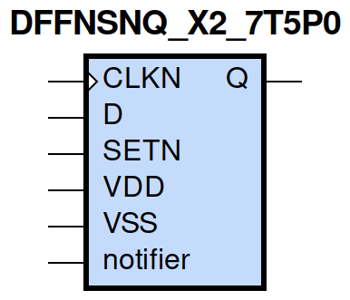
gf180mcu_fd_sc_mcu7t5v0__dffnsnq_2 symbol
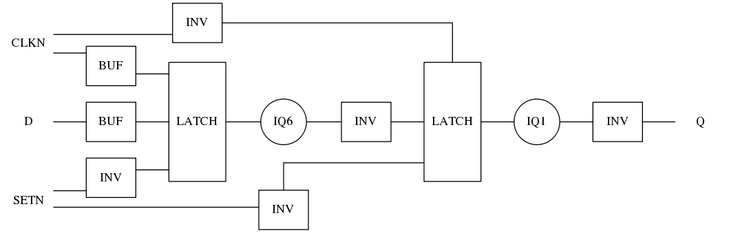
gf180mcu_fd_sc_mcu7t5v0__dffnsnq_2 schematic

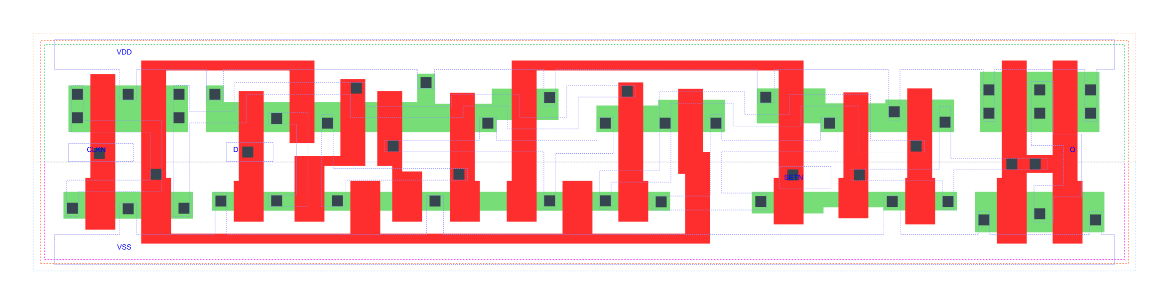
gf180mcu_fd_sc_mcu7t5v0__dffnsnq_2 layout
DFFNSNQ_X2 is a negative edge triggered D-type flip flop, active low set and 2X drive strength
Attribute |
Value |
area |
83.417600 µm2 |
TRUTH TABLE
Input |
Output |
||
SETN |
D |
CLKN |
Q |
H |
L |
↓ |
L |
H |
H |
↓ |
H |
L |
X |
X |
H |
Constraint Pin |
Related Pin |
setup(ns) |
hold(ns) |
D(HL) |
CLKN(HL) |
0.3320 |
0.0230 |
D(LH) |
CLKN(HL) |
0.2290 |
0.1370 |
Constraint Pin |
Related Pin |
recovery(ns) |
removal(ns) |
SETN(LH) |
CLKN(HL) |
0.1030 |
0.1140 |
Constraint Pin |
Related Pin |
Minimum Pulse Width(ns) |
CLKN(LHL) |
CLKN(LH) |
0.4610 |
CLKN(LHL) |
CLKN(LH) |
0.4310 |
CLKN(HLH) |
CLKN(HL) |
0.4760 |
CLKN(HLH) |
CLKN(HL) |
0.4850 |
SETN(HLH) |
SETN(HL) |
0.3880 |
SETN(HLH) |
SETN(HL) |
0.3880 |
SETN(HLH) |
SETN(HL) |
0.3880 |
SETN(HLH) |
SETN(HL) |
0.3880 |
Pin |
Type |
Capacitance (pf) |
CLKN |
input |
0.0038 |
D |
input |
0.0026 |
SETN |
input |
0.0064 |
Input Pin |
Output |
When Condition |
Tin (ns) |
Out Load (pf) |
Delay (ns) |
Tout (ns) |
CLKN(HL) |
Q(LH) |
D&SETN |
0.0100 |
0.0010 |
0.7110 |
0.0431 |
CLKN(HL) |
Q(HL) |
!D&SETN |
0.0100 |
0.0010 |
0.6654 |
0.0486 |
SETN(HL) |
Q(LH) |
!CLKN&!D |
0.0100 |
0.0010 |
0.5939 |
0.0419 |
SETN(HL) |
Q(LH) |
CLKN&!D |
0.0100 |
0.0010 |
0.5331 |
0.0413 |
SETN(HL) |
Q(LH) |
!CLKN&D |
0.0100 |
0.0010 |
0.5939 |
0.0418 |
SETN(HL) |
Q(LH) |
CLKN&D |
0.0100 |
0.0010 |
0.5334 |
0.0417 |
Input Pin |
When Condition |
Tin (ns) |
Output |
Out Load (pf) |
Energy (uW/MHz) |
SETN |
!CLKN&!D |
0.0100 |
Q(LH) |
0.0010 |
0.7160 |
SETN |
CLKN&!D |
0.0100 |
Q(LH) |
0.0010 |
0.6351 |
SETN |
!CLKN&D |
0.0100 |
Q(LH) |
0.0010 |
0.7160 |
SETN |
CLKN&D |
0.0100 |
Q(LH) |
0.0010 |
0.5386 |
CLKN |
D&SETN |
0.0100 |
Q(LH) |
0.0010 |
0.8951 |
CLKN |
!D&SETN |
0.0100 |
Q(HL) |
0.0010 |
0.8245 |
SETN(HL) |
!CLKN&!D |
0.0100 |
n/a |
n/a |
0.0473 |
SETN(HL) |
CLKN&!D |
0.0100 |
n/a |
n/a |
0.1425 |
SETN(HL) |
!CLKN&D |
0.0100 |
n/a |
n/a |
0.0473 |
SETN(HL) |
CLKN&D |
0.0100 |
n/a |
n/a |
0.0472 |
CLKN(LH) |
!D&!SETN |
0.0100 |
n/a |
n/a |
0.3092 |
CLKN(LH) |
D&!SETN |
0.0100 |
n/a |
n/a |
0.2258 |
CLKN(LH) |
!D&SETN |
0.0100 |
n/a |
n/a |
0.2240 |
CLKN(LH) |
D&SETN |
0.0100 |
n/a |
n/a |
0.2258 |
CLKN(HL) |
!D&!SETN |
0.0100 |
n/a |
n/a |
0.3753 |
CLKN(HL) |
D&!SETN |
0.0100 |
n/a |
n/a |
0.3241 |
CLKN(HL) |
!D&SETN |
0.0100 |
n/a |
n/a |
0.3190 |
CLKN(HL) |
D&SETN |
0.0100 |
n/a |
n/a |
0.3240 |
D(HL) |
!CLKN&!SETN |
0.0100 |
n/a |
n/a |
0.0609 |
D(HL) |
CLKN&!SETN |
0.0100 |
n/a |
n/a |
0.1478 |
D(HL) |
!CLKN&SETN |
0.0100 |
n/a |
n/a |
0.0609 |
D(HL) |
CLKN&SETN |
0.0100 |
n/a |
n/a |
0.2183 |
D(LH) |
!CLKN&!SETN |
0.0100 |
n/a |
n/a |
0.0053 |
D(LH) |
CLKN&!SETN |
0.0100 |
n/a |
n/a |
0.0537 |
D(LH) |
!CLKN&SETN |
0.0100 |
n/a |
n/a |
0.0054 |
D(LH) |
CLKN&SETN |
0.0100 |
n/a |
n/a |
0.1750 |
SETN(LH) |
!CLKN&!D |
0.0100 |
n/a |
n/a |
-0.0251 |
SETN(LH) |
!CLKN&D |
0.0100 |
n/a |
n/a |
-0.0251 |
SETN(LH) |
CLKN&!D |
0.0100 |
n/a |
n/a |
0.0304 |
SETN(LH) |
CLKN&D |
0.0100 |
n/a |
n/a |
-0.0252 |
When Condition |
Power (nW) |
!CLKN&!D&!SETN |
0.4718 |
!CLKN&D&!SETN |
0.4704 |
CLKN&!D&!SETN |
0.4349 |
CLKN&D&!SETN |
0.4322 |
!CLKN&!D&SETN |
0.5572 |
CLKN&!D&SETN |
0.6398 |
CLKN&D&SETN |
0.6296 |
!CLKN&D&SETN |
0.6633 |