gf180mcu_fd_sc_mcu7t5v0__invz_x16
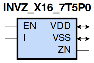
gf180mcu_fd_sc_mcu7t5v0__invz_x16 symbol
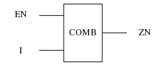
gf180mcu_fd_sc_mcu7t5v0__invz_x16 schematic

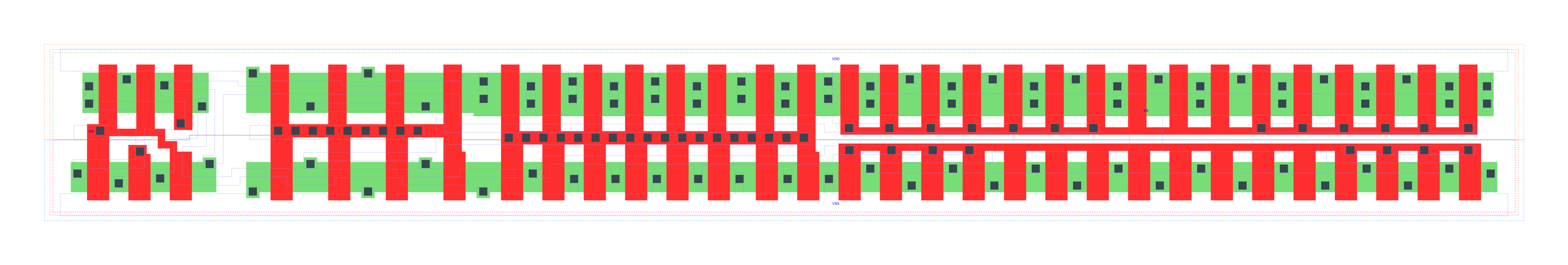
gf180mcu_fd_sc_mcu7t5v0__invz_x16 layout
INVZ_X16 is a tri-state inverter, 16X drive strength
Attribute |
Value |
area |
153.664000 µm2 |
Output Pin |
Function |
ZN |
(!I) |
EN |
I |
ZN |
1 |
0 |
1 |
1 |
1 |
0 |
0 |
? |
z |
Pin |
Type |
Capacitance (pf) |
EN |
input |
0.0090 |
I |
input |
0.0181 |
Input Pin |
Output |
When Condition |
Tin (ns) |
Out Load (pf) |
Delay (ns) |
Tout (ns) |
EN(LH) |
ZN(ZL) |
I |
0.0100 |
0.0010 |
0.2097 |
0.0527 |
EN(LH) |
ZN(ZH) |
!I |
0.0100 |
0.0010 |
0.2621 |
0.0648 |
EN(HL) |
ZN(HZ) |
!I |
0.0100 |
0.6750 |
0.0000 |
|
EN(HL) |
ZN(LZ) |
I |
0.0100 |
0.4670 |
0.0000 |
|
I(LH) |
ZN(HL) |
EN |
0.0100 |
0.0010 |
0.3480 |
0.0505 |
I(HL) |
ZN(LH) |
EN |
0.0100 |
0.0010 |
0.4443 |
0.0616 |
Input Pin |
When Condition |
Tin (ns) |
Output |
Out Load (pf) |
Energy (uW/MHz) |
I |
EN |
0.0100 |
ZN(HL) |
0.0010 |
2.3424 |
I |
EN |
0.0100 |
ZN(LH) |
0.0010 |
2.3656 |
EN |
I |
0.0100 |
ZN(HL) |
0.0010 |
1.4016 |
EN(HL) |
I |
0.0100 |
n/a |
n/a |
0.2490 |
EN(HL) |
!I |
0.0100 |
n/a |
n/a |
0.6917 |
EN |
!I |
0.0100 |
ZN(LH) |
0.0010 |
1.3432 |
I(LH) |
!EN |
0.0100 |
n/a |
n/a |
0.2972 |
I(HL) |
!EN |
0.0100 |
n/a |
n/a |
0.8016 |
When Condition |
Power (nW) |
!EN&!I |
0.4362 |
!EN&I |
0.4401 |
EN&!I |
0.8735 |
EN&I |
0.8846 |