gf180mcu_fd_sc_mcu7t5v0__oai21_2
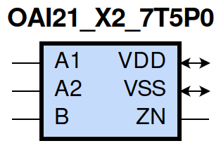
gf180mcu_fd_sc_mcu7t5v0__oai21_2 symbol
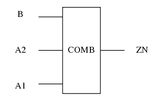
gf180mcu_fd_sc_mcu7t5v0__oai21_2 schematic

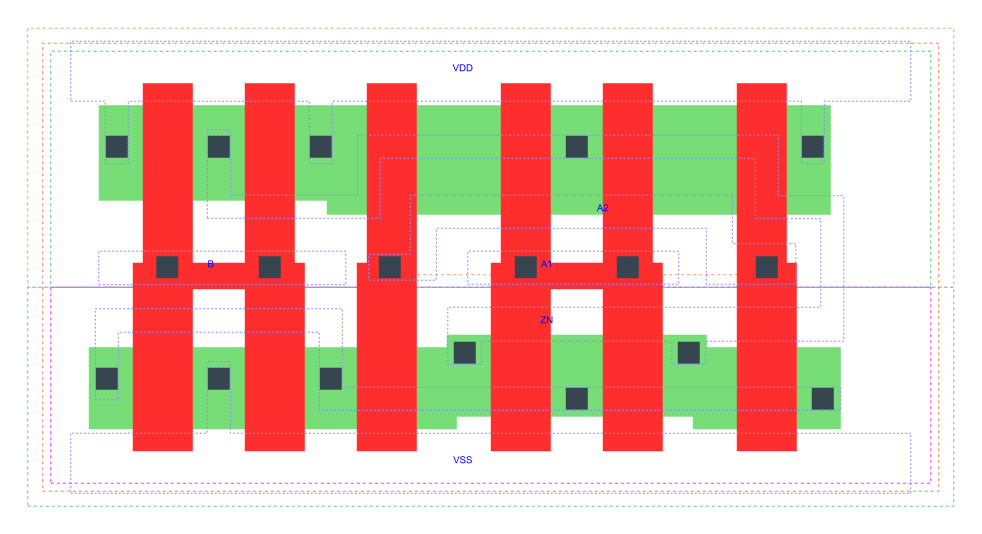
gf180mcu_fd_sc_mcu7t5v0__oai21_2 layout
OAI21_X2 is a 2-input OR into 2-input NAND, NAND[OR(A1,A2),B], 2X drive strength
Attribute |
Value |
area |
32.928000 µm2 |
Output Pin |
Function |
ZN |
(((!A1)&(!A2))|(!B)) |
A1 |
A2 |
B |
ZN |
0 |
0 |
? |
1 |
? |
? |
0 |
1 |
1 |
? |
1 |
0 |
? |
1 |
1 |
0 |
Pin |
Type |
Capacitance (pf) |
B |
input |
0.0085 |
A2 |
input |
0.0095 |
A1 |
input |
0.0091 |
Input Pin |
Output |
When Condition |
Tin (ns) |
Out Load (pf) |
Delay (ns) |
Tout (ns) |
B(LH) |
ZN(HL) |
!A1&A2 |
0.0100 |
0.0010 |
0.1064 |
0.0541 |
B(LH) |
ZN(HL) |
A1&!A2 |
0.0100 |
0.0010 |
0.0847 |
0.0386 |
B(LH) |
ZN(HL) |
A1&A2 |
0.0100 |
0.0010 |
0.0730 |
0.0366 |
B(HL) |
ZN(LH) |
!A1&A2 |
0.0100 |
0.0010 |
0.1295 |
0.1168 |
B(HL) |
ZN(LH) |
A1&!A2 |
0.0100 |
0.0010 |
0.1227 |
0.0891 |
B(HL) |
ZN(LH) |
A1&A2 |
0.0100 |
0.0010 |
0.1400 |
0.1014 |
A2(HL) |
ZN(LH) |
!A1&B |
0.0100 |
0.0010 |
0.1475 |
0.0899 |
A2(LH) |
ZN(HL) |
!A1&B |
0.0100 |
0.0010 |
0.0796 |
0.0545 |
A1(HL) |
ZN(LH) |
!A2&B |
0.0100 |
0.0010 |
0.1184 |
0.0896 |
A1(LH) |
ZN(HL) |
!A2&B |
0.0100 |
0.0010 |
0.0603 |
0.0380 |
Input Pin |
When Condition |
Tin (ns) |
Output |
Out Load (pf) |
Energy (uW/MHz) |
A1 |
!A2&B |
0.0100 |
ZN(LH) |
0.0010 |
0.2649 |
B |
!A1&A2 |
0.0100 |
ZN(HL) |
0.0010 |
0.0640 |
B |
A1&!A2 |
0.0100 |
ZN(HL) |
0.0010 |
0.0080 |
B |
A1&A2 |
0.0100 |
ZN(HL) |
0.0010 |
0.0081 |
A2 |
!A1&B |
0.0100 |
ZN(LH) |
0.0010 |
0.3191 |
A1 |
!A2&B |
0.0100 |
ZN(HL) |
0.0010 |
0.0067 |
B |
!A1&A2 |
0.0100 |
ZN(LH) |
0.0010 |
0.4705 |
B |
A1&!A2 |
0.0100 |
ZN(LH) |
0.0010 |
0.4164 |
B |
A1&A2 |
0.0100 |
ZN(LH) |
0.0010 |
0.4613 |
A2 |
!A1&B |
0.0100 |
ZN(HL) |
0.0010 |
0.0577 |
B(HL) |
!A1&!A2 |
0.0100 |
n/a |
n/a |
0.0717 |
A2(LH) |
!A1&!B |
0.0100 |
n/a |
n/a |
0.0324 |
A2(LH) |
A1&!B |
0.0100 |
n/a |
n/a |
-0.0770 |
A2(LH) |
A1&B |
0.0100 |
n/a |
n/a |
-0.0584 |
A1(LH) |
!A2&!B |
0.0100 |
n/a |
n/a |
0.0318 |
A1(LH) |
A2&!B |
0.0100 |
n/a |
n/a |
-0.0779 |
A1(LH) |
A2&B |
0.0100 |
n/a |
n/a |
-0.0203 |
A2(HL) |
!A1&!B |
0.0100 |
n/a |
n/a |
0.0795 |
A2(HL) |
A1&!B |
0.0100 |
n/a |
n/a |
0.0826 |
A2(HL) |
A1&B |
0.0100 |
n/a |
n/a |
0.0704 |
B(LH) |
!A1&!A2 |
0.0100 |
n/a |
n/a |
-0.0616 |
A1(HL) |
!A2&!B |
0.0100 |
n/a |
n/a |
0.0799 |
A1(HL) |
A2&!B |
0.0100 |
n/a |
n/a |
0.0829 |
A1(HL) |
A2&B |
0.0100 |
n/a |
n/a |
0.0585 |
When Condition |
Power (nW) |
!A1&!A2&!B |
0.1508 |
!A1&!A2&B |
0.1518 |
!A1&A2&!B |
0.2704 |
A1&!A2&!B |
0.2704 |
A1&A2&!B |
0.2710 |
!A1&A2&B |
0.2269 |
A1&!A2&B |
0.1555 |
A1&A2&B |
0.1555 |