gf180mcu_fd_sc_mcu7t5v0__xor3_2
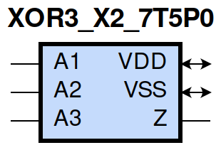
gf180mcu_fd_sc_mcu7t5v0__xor3_2 symbol
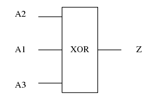
gf180mcu_fd_sc_mcu7t5v0__xor3_2 schematic

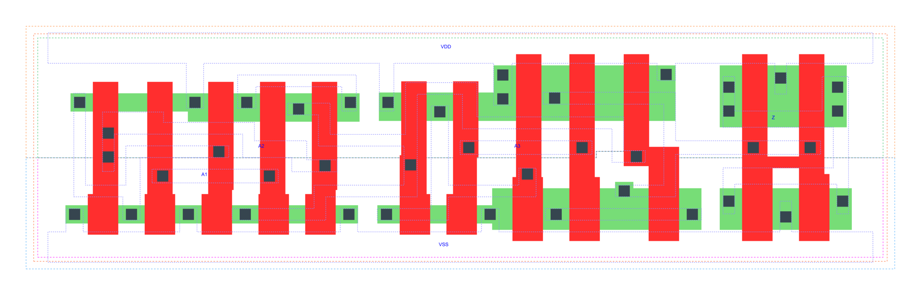
gf180mcu_fd_sc_mcu7t5v0__xor3_2 layout
XOR3_X2 is a 3-input exclusive OR, 2X drive strength
Attribute |
Value |
area |
63.660800 µm2 |
Output Pin |
Function |
Z |
(A1^A2^A3) |
A1 |
A2 |
A3 |
Z |
1 |
1 |
1 |
1 |
1 |
0 |
0 |
1 |
0 |
1 |
0 |
1 |
0 |
0 |
1 |
1 |
1 |
1 |
0 |
0 |
1 |
0 |
1 |
0 |
0 |
1 |
1 |
0 |
0 |
0 |
0 |
0 |
Pin |
Type |
Capacitance (pf) |
A2 |
input |
0.0052 |
A1 |
input |
0.0048 |
A3 |
input |
0.0069 |
Input Pin |
Output |
When Condition |
Tin (ns) |
Out Load (pf) |
Delay (ns) |
Tout (ns) |
A2(HL) |
Z(HL) |
!A1&!A3 |
0.0100 |
0.0010 |
0.8916 |
0.0576 |
A2(HL) |
Z(HL) |
A1&A3 |
0.0100 |
0.0010 |
0.9310 |
0.0472 |
A2(LH) |
Z(LH) |
!A1&!A3 |
0.0100 |
0.0010 |
0.8376 |
0.0513 |
A2(LH) |
Z(LH) |
A1&A3 |
0.0100 |
0.0010 |
0.6710 |
0.0457 |
A2(HL) |
Z(LH) |
!A1&A3 |
0.0100 |
0.0010 |
0.9842 |
0.0457 |
A2(HL) |
Z(LH) |
A1&!A3 |
0.0100 |
0.0010 |
0.7345 |
0.0517 |
A2(LH) |
Z(HL) |
!A1&A3 |
0.0100 |
0.0010 |
1.0339 |
0.0472 |
A2(LH) |
Z(HL) |
A1&!A3 |
0.0100 |
0.0010 |
0.5782 |
0.0584 |
A1(LH) |
Z(HL) |
!A2&A3 |
0.0100 |
0.0010 |
1.0768 |
0.0475 |
A1(LH) |
Z(HL) |
A2&!A3 |
0.0100 |
0.0010 |
0.5670 |
0.0584 |
A1(HL) |
Z(LH) |
!A2&A3 |
0.0100 |
0.0010 |
1.0147 |
0.0457 |
A1(HL) |
Z(LH) |
A2&!A3 |
0.0100 |
0.0010 |
0.7010 |
0.0511 |
A1(LH) |
Z(LH) |
!A2&!A3 |
0.0100 |
0.0010 |
0.8804 |
0.0520 |
A1(LH) |
Z(LH) |
A2&A3 |
0.0100 |
0.0010 |
0.6598 |
0.0457 |
A1(HL) |
Z(HL) |
!A2&!A3 |
0.0100 |
0.0010 |
0.9220 |
0.0577 |
A1(HL) |
Z(HL) |
A2&A3 |
0.0100 |
0.0010 |
0.8972 |
0.0471 |
A3(LH) |
Z(LH) |
!A1&!A2 |
0.0100 |
0.0010 |
0.2106 |
0.0446 |
A3(LH) |
Z(LH) |
A1&A2 |
0.0100 |
0.0010 |
0.2106 |
0.0446 |
A3(HL) |
Z(LH) |
!A1&A2 |
0.0100 |
0.0010 |
0.4393 |
0.0471 |
A3(HL) |
Z(LH) |
A1&!A2 |
0.0100 |
0.0010 |
0.4392 |
0.0472 |
A3(HL) |
Z(HL) |
!A1&!A2 |
0.0100 |
0.0010 |
0.3086 |
0.0573 |
A3(HL) |
Z(HL) |
A1&A2 |
0.0100 |
0.0010 |
0.3084 |
0.0572 |
A3(LH) |
Z(HL) |
!A1&A2 |
0.0100 |
0.0010 |
0.4390 |
0.0473 |
A3(LH) |
Z(HL) |
A1&!A2 |
0.0100 |
0.0010 |
0.4389 |
0.0474 |
Input Pin |
When Condition |
Tin (ns) |
Output |
Out Load (pf) |
Energy (uW/MHz) |
A3 |
!A1&!A2 |
0.0100 |
Z(LH) |
0.0010 |
0.2308 |
A3 |
A1&A2 |
0.0100 |
Z(LH) |
0.0010 |
0.2308 |
A3 |
!A1&A2 |
0.0100 |
Z(LH) |
0.0010 |
0.5173 |
A3 |
A1&!A2 |
0.0100 |
Z(LH) |
0.0010 |
0.5170 |
A2 |
!A1&!A3 |
0.0100 |
Z(HL) |
0.0010 |
0.6800 |
A2 |
A1&A3 |
0.0100 |
Z(HL) |
0.0010 |
0.7795 |
A2 |
!A1&A3 |
0.0100 |
Z(HL) |
0.0010 |
0.7736 |
A2 |
A1&!A3 |
0.0100 |
Z(HL) |
0.0010 |
0.5064 |
A1 |
!A2&A3 |
0.0100 |
Z(HL) |
0.0010 |
0.8031 |
A1 |
A2&!A3 |
0.0100 |
Z(HL) |
0.0010 |
0.4997 |
A1 |
!A2&!A3 |
0.0100 |
Z(HL) |
0.0010 |
0.6908 |
A1 |
A2&A3 |
0.0100 |
Z(HL) |
0.0010 |
0.7604 |
A2 |
!A1&!A3 |
0.0100 |
Z(LH) |
0.0010 |
0.6270 |
A2 |
A1&A3 |
0.0100 |
Z(LH) |
0.0010 |
0.4724 |
A2 |
!A1&A3 |
0.0100 |
Z(LH) |
0.0010 |
0.6490 |
A2 |
A1&!A3 |
0.0100 |
Z(LH) |
0.0010 |
0.6390 |
A1 |
!A2&A3 |
0.0100 |
Z(LH) |
0.0010 |
0.6596 |
A1 |
A2&!A3 |
0.0100 |
Z(LH) |
0.0010 |
0.6141 |
A1 |
!A2&!A3 |
0.0100 |
Z(LH) |
0.0010 |
0.6624 |
A1 |
A2&A3 |
0.0100 |
Z(LH) |
0.0010 |
0.4656 |
A3 |
!A1&!A2 |
0.0100 |
Z(HL) |
0.0010 |
0.4674 |
A3 |
A1&A2 |
0.0100 |
Z(HL) |
0.0010 |
0.4674 |
A3 |
!A1&A2 |
0.0100 |
Z(HL) |
0.0010 |
0.4926 |
A3 |
A1&!A2 |
0.0100 |
Z(HL) |
0.0010 |
0.4927 |
When Condition |
Power (nW) |
!A1&!A2&!A3 |
0.3401 |
!A1&A2&A3 |
0.3468 |
A1&!A2&A3 |
0.4232 |
A1&A2&!A3 |
0.2576 |
!A1&!A2&A3 |
0.3419 |
!A1&A2&!A3 |
0.3383 |
A1&!A2&!A3 |
0.4148 |
A1&A2&A3 |
0.2595 |