gf180mcu_fd_sc_mcu7t5v0__xnor2_2
gf180mcu_fd_sc_mcu7t5v0__xnor2_2 symbol
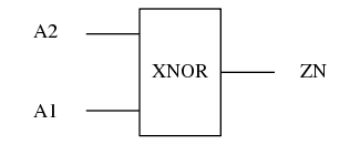
gf180mcu_fd_sc_mcu7t5v0__xnor2_2 schematic

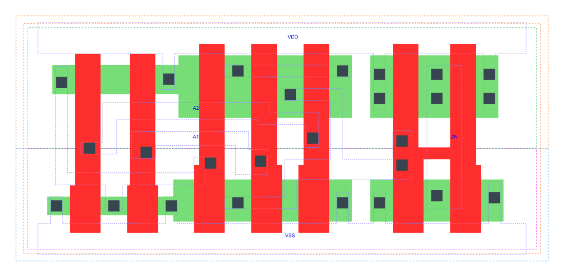
gf180mcu_fd_sc_mcu7t5v0__xnor2_2 layout
XNOR2_X2 is a 2-input exclusive NOR, 2X drive strength
Attribute |
Value |
area |
37.318400 µm2 |
Output Pin |
Function |
ZN |
(!(A1^A2)) |
A1 |
A2 |
ZN |
1 |
1 |
1 |
0 |
0 |
1 |
1 |
0 |
0 |
0 |
1 |
0 |
Pin |
Type |
Capacitance (pf) |
A2 |
input |
0.0074 |
A1 |
input |
0.0075 |
Input Pin |
Output |
When Condition |
Tin (ns) |
Out Load (pf) |
Delay (ns) |
Tout (ns) |
A2(LH) |
ZN(LH) |
A1 |
0.0100 |
0.0010 |
0.2069 |
0.0361 |
A2(HL) |
ZN(LH) |
!A1 |
0.0100 |
0.0010 |
0.5024 |
0.0345 |
A2(HL) |
ZN(HL) |
A1 |
0.0100 |
0.0010 |
0.2820 |
0.0502 |
A2(LH) |
ZN(HL) |
!A1 |
0.0100 |
0.0010 |
0.3934 |
0.0455 |
A1(HL) |
ZN(LH) |
!A2 |
0.0100 |
0.0010 |
0.5312 |
0.0347 |
A1(HL) |
ZN(HL) |
A2 |
0.0100 |
0.0010 |
0.2541 |
0.0454 |
A1(LH) |
ZN(HL) |
!A2 |
0.0100 |
0.0010 |
0.4432 |
0.0500 |
A1(LH) |
ZN(LH) |
A2 |
0.0100 |
0.0010 |
0.1954 |
0.0361 |
Input Pin |
When Condition |
Tin (ns) |
Output |
Out Load (pf) |
Energy (uW/MHz) |
A2 |
A1 |
0.0100 |
ZN(LH) |
0.0010 |
0.2058 |
A2 |
!A1 |
0.0100 |
ZN(LH) |
0.0010 |
0.4985 |
A1 |
!A2 |
0.0100 |
ZN(LH) |
0.0010 |
0.5156 |
A1 |
A2 |
0.0100 |
ZN(LH) |
0.0010 |
0.1957 |
A1 |
A2 |
0.0100 |
ZN(HL) |
0.0010 |
0.4303 |
A1 |
!A2 |
0.0100 |
ZN(HL) |
0.0010 |
0.5152 |
A2 |
A1 |
0.0100 |
ZN(HL) |
0.0010 |
0.4818 |
A2 |
!A1 |
0.0100 |
ZN(HL) |
0.0010 |
0.4432 |
When Condition |
Power (nW) |
!A1&!A2 |
0.2613 |
A1&A2 |
0.1800 |
!A1&A2 |
0.1800 |
A1&!A2 |
0.2559 |