gf180mcu_fd_sc_mcu7t5v0__bufz_x16
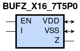
gf180mcu_fd_sc_mcu7t5v0__bufz_x16 symbol
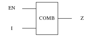
gf180mcu_fd_sc_mcu7t5v0__bufz_x16 schematic

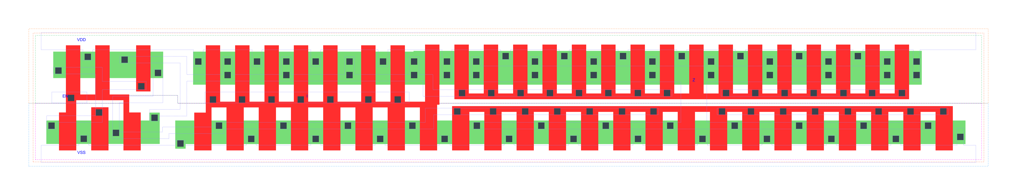
gf180mcu_fd_sc_mcu7t5v0__bufz_x16 layout
BUFZ_X16 is a tri-state buffer, 16X drive strength | | Attributes
Attribute |
Value |
area |
127.321600 µm2 |
Output Pin |
Function |
Z |
I |
EN |
I |
Z |
1 |
1 |
1 |
1 |
0 |
0 |
0 |
? |
z |
Pin |
Type |
Capacitance (pf) |
EN |
input |
0.0083 |
I |
input |
0.0353 |
Input Pin |
Output |
When Condition |
Tin (ns) |
Out Load (pf) |
Delay (ns) |
Tout (ns) |
EN(LH) |
Z(ZL) |
!I |
0.0100 |
0.0010 |
0.2074 |
0.0538 |
EN(LH) |
Z(ZH) |
I |
0.0100 |
0.0010 |
0.2545 |
0.0629 |
EN(HL) |
Z(LZ) |
!I |
0.0100 |
0.4710 |
0.0000 |
|
EN(HL) |
Z(HZ) |
I |
0.0100 |
0.7580 |
0.0000 |
|
I(HL) |
Z(HL) |
EN |
0.0100 |
0.0010 |
0.2659 |
0.0509 |
I(LH) |
Z(LH) |
EN |
0.0100 |
0.0010 |
0.3199 |
0.0587 |
Input Pin |
When Condition |
Tin (ns) |
Output |
Out Load (pf) |
Energy (uW/MHz) |
I |
EN |
0.0100 |
Z(HL) |
0.0010 |
2.2575 |
I |
EN |
0.0100 |
Z(LH) |
0.0010 |
1.2261 |
EN(HL) |
!I |
0.0100 |
n/a |
n/a |
0.2259 |
EN(HL) |
I |
0.0100 |
n/a |
n/a |
0.6459 |
I(LH) |
!EN |
0.0100 |
n/a |
n/a |
-0.2961 |
EN |
I |
0.0100 |
Z(LH) |
0.0010 |
1.3076 |
I(HL) |
!EN |
0.0100 |
n/a |
n/a |
0.2972 |
EN |
!I |
0.0100 |
Z(HL) |
0.0010 |
1.3619 |
When Condition |
Power (nW) |
!EN&!I |
0.3339 |
!EN&I |
0.3339 |
EN&!I |
0.7788 |
EN&I |
0.7714 |