gf180mcu_fd_sc_mcu7t5v0__oai21_1
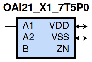
gf180mcu_fd_sc_mcu7t5v0__oai21_1 symbol
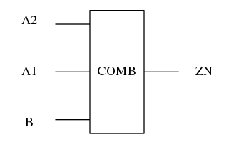
gf180mcu_fd_sc_mcu7t5v0__oai21_1 schematic

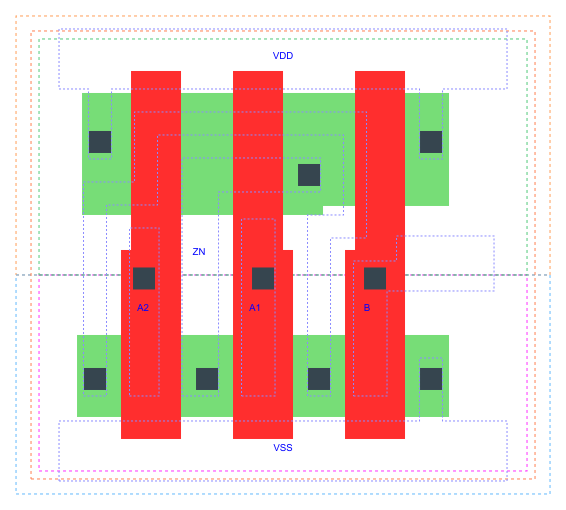
gf180mcu_fd_sc_mcu7t5v0__oai21_1 layout
OAI21_X1 is a 2-input OR into 2-input NAND, NAND[OR(A1,A2),B], 1X drive strength
Attribute |
Value |
area |
17.561600 µm2 |
Output Pin |
Function |
ZN |
(((!A1)&(!A2))|(!B)) |
A1 |
A2 |
B |
ZN |
0 |
0 |
? |
1 |
? |
? |
0 |
1 |
1 |
? |
1 |
0 |
? |
1 |
1 |
0 |
Pin |
Type |
Capacitance (pf) |
A2 |
input |
0.0048 |
A1 |
input |
0.0050 |
B |
input |
0.0048 |
Input Pin |
Output |
When Condition |
Tin (ns) |
Out Load (pf) |
Delay (ns) |
Tout (ns) |
A2(HL) |
ZN(LH) |
!A1&B |
0.0100 |
0.0010 |
0.1359 |
0.0852 |
A2(LH) |
ZN(HL) |
!A1&B |
0.0100 |
0.0010 |
0.0836 |
0.0565 |
A1(HL) |
ZN(LH) |
!A2&B |
0.0100 |
0.0010 |
0.1115 |
0.0848 |
A1(LH) |
ZN(HL) |
!A2&B |
0.0100 |
0.0010 |
0.0633 |
0.0398 |
B(LH) |
ZN(HL) |
!A1&A2 |
0.0100 |
0.0010 |
0.1179 |
0.0564 |
B(LH) |
ZN(HL) |
A1&!A2 |
0.0100 |
0.0010 |
0.0949 |
0.0409 |
B(LH) |
ZN(HL) |
A1&A2 |
0.0100 |
0.0010 |
0.0814 |
0.0392 |
B(HL) |
ZN(LH) |
!A1&A2 |
0.0100 |
0.0010 |
0.1198 |
0.1084 |
B(HL) |
ZN(LH) |
A1&!A2 |
0.0100 |
0.0010 |
0.1130 |
0.0836 |
B(HL) |
ZN(LH) |
A1&A2 |
0.0100 |
0.0010 |
0.1295 |
0.0949 |
Input Pin |
When Condition |
Tin (ns) |
Output |
Out Load (pf) |
Energy (uW/MHz) |
A1 |
!A2&B |
0.0100 |
ZN(LH) |
0.0010 |
0.1224 |
B |
!A1&A2 |
0.0100 |
ZN(HL) |
0.0010 |
0.0335 |
B |
A1&!A2 |
0.0100 |
ZN(HL) |
0.0010 |
0.0086 |
B |
A1&A2 |
0.0100 |
ZN(HL) |
0.0010 |
0.0086 |
A2 |
!A1&B |
0.0100 |
ZN(LH) |
0.0010 |
0.1524 |
A1 |
!A2&B |
0.0100 |
ZN(HL) |
0.0010 |
0.0094 |
B |
!A1&A2 |
0.0100 |
ZN(LH) |
0.0010 |
0.2483 |
B |
A1&!A2 |
0.0100 |
ZN(LH) |
0.0010 |
0.2185 |
B |
A1&A2 |
0.0100 |
ZN(LH) |
0.0010 |
0.2411 |
A2 |
!A1&B |
0.0100 |
ZN(HL) |
0.0010 |
0.0311 |
B(HL) |
!A1&!A2 |
0.0100 |
n/a |
n/a |
0.0410 |
A2(LH) |
!A1&!B |
0.0100 |
n/a |
n/a |
0.0305 |
A2(LH) |
A1&!B |
0.0100 |
n/a |
n/a |
-0.0426 |
A2(LH) |
A1&B |
0.0100 |
n/a |
n/a |
-0.0329 |
A1(LH) |
!A2&!B |
0.0100 |
n/a |
n/a |
0.0300 |
A1(LH) |
A2&!B |
0.0100 |
n/a |
n/a |
-0.0431 |
A1(LH) |
A2&B |
0.0100 |
n/a |
n/a |
-0.0111 |
A2(HL) |
!A1&!B |
0.0100 |
n/a |
n/a |
0.0441 |
A2(HL) |
A1&!B |
0.0100 |
n/a |
n/a |
0.0446 |
A2(HL) |
A1&B |
0.0100 |
n/a |
n/a |
0.0392 |
B(LH) |
!A1&!A2 |
0.0100 |
n/a |
n/a |
-0.0367 |
A1(HL) |
!A2&!B |
0.0100 |
n/a |
n/a |
0.0443 |
A1(HL) |
A2&!B |
0.0100 |
n/a |
n/a |
0.0447 |
A1(HL) |
A2&B |
0.0100 |
n/a |
n/a |
0.0264 |
When Condition |
Power (nW) |
!A1&!A2&!B |
0.1004 |
!A1&!A2&B |
0.1009 |
!A1&A2&!B |
0.1596 |
A1&!A2&!B |
0.1596 |
A1&A2&!B |
0.1599 |
!A1&A2&B |
0.1386 |
A1&!A2&B |
0.1029 |
A1&A2&B |
0.1029 |