gf180mcu_fd_sc_mcu7t5v0__xor2_2
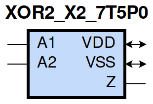
gf180mcu_fd_sc_mcu7t5v0__xor2_2 symbol
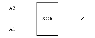
gf180mcu_fd_sc_mcu7t5v0__xor2_2 schematic

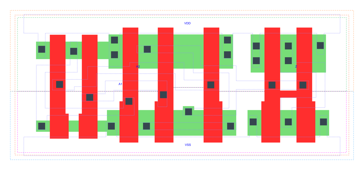
gf180mcu_fd_sc_mcu7t5v0__xor2_2 layout
XOR2_X2 is a 2-input exclusive OR, 2X drive strength
Attribute |
Value |
area |
39.513600 µm2 |
Output Pin |
Function |
Z |
(A1^A2) |
A1 |
A2 |
Z |
1 |
0 |
1 |
0 |
1 |
1 |
1 |
1 |
0 |
0 |
0 |
0 |
Pin |
Type |
Capacitance (pf) |
A2 |
input |
0.0073 |
A1 |
input |
0.0072 |
Input Pin |
Output |
When Condition |
Tin (ns) |
Out Load (pf) |
Delay (ns) |
Tout (ns) |
A2(HL) |
Z(HL) |
!A1 |
0.0100 |
0.0010 |
0.3279 |
0.0509 |
A2(LH) |
Z(LH) |
!A1 |
0.0100 |
0.0010 |
0.2313 |
0.0397 |
A2(HL) |
Z(LH) |
A1 |
0.0100 |
0.0010 |
0.3913 |
0.0387 |
A2(LH) |
Z(HL) |
A1 |
0.0100 |
0.0010 |
0.4186 |
0.0422 |
A1(LH) |
Z(HL) |
A2 |
0.0100 |
0.0010 |
0.4310 |
0.0422 |
A1(HL) |
Z(LH) |
A2 |
0.0100 |
0.0010 |
0.4353 |
0.0403 |
A1(LH) |
Z(LH) |
!A2 |
0.0100 |
0.0010 |
0.2008 |
0.0378 |
A1(HL) |
Z(HL) |
!A2 |
0.0100 |
0.0010 |
0.2967 |
0.0511 |
Input Pin |
When Condition |
Tin (ns) |
Output |
Out Load (pf) |
Energy (uW/MHz) |
A2 |
!A1 |
0.0100 |
Z(HL) |
0.0010 |
0.4901 |
A2 |
A1 |
0.0100 |
Z(HL) |
0.0010 |
0.4775 |
A1 |
A2 |
0.0100 |
Z(HL) |
0.0010 |
0.5002 |
A1 |
!A2 |
0.0100 |
Z(HL) |
0.0010 |
0.4622 |
A2 |
!A1 |
0.0100 |
Z(LH) |
0.0010 |
0.2543 |
A2 |
A1 |
0.0100 |
Z(LH) |
0.0010 |
0.4423 |
A1 |
A2 |
0.0100 |
Z(LH) |
0.0010 |
0.4916 |
A1 |
!A2 |
0.0100 |
Z(LH) |
0.0010 |
0.2097 |
When Condition |
Power (nW) |
!A1&!A2 |
0.1795 |
A1&A2 |
0.2657 |
!A1&A2 |
0.2572 |
A1&!A2 |
0.1813 |