gf180mcu_fd_sc_mcu7t5v0__or2_2
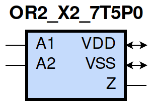
gf180mcu_fd_sc_mcu7t5v0__or2_2 symbol
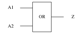
gf180mcu_fd_sc_mcu7t5v0__or2_2 schematic

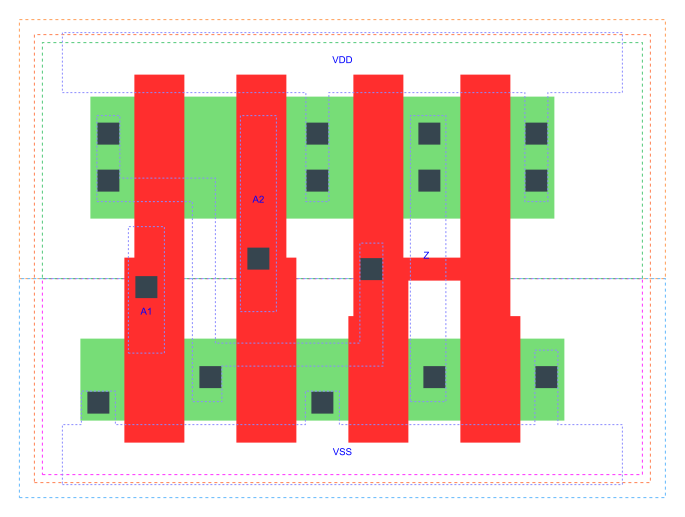
gf180mcu_fd_sc_mcu7t5v0__or2_2 layout
OR2_X2 is a 2-input OR(A1,A2), 2X drive strength
Attribute |
Value |
area |
21.952000 µm2 |
Output Pin |
Function |
Z |
(A1|A2) |
A1 |
A2 |
Z |
1 |
? |
1 |
? |
1 |
1 |
0 |
0 |
0 |
Pin |
Type |
Capacitance (pf) |
A1 |
input |
0.0048 |
A2 |
input |
0.0048 |
Input Pin |
Output |
When Condition |
Tin (ns) |
Out Load (pf) |
Delay (ns) |
Tout (ns) |
A1(LH) |
Z(LH) |
!A2 |
0.0100 |
0.0010 |
0.1372 |
0.0278 |
A1(HL) |
Z(HL) |
!A2 |
0.0100 |
0.0010 |
0.2463 |
0.0435 |
A2(HL) |
Z(HL) |
!A1 |
0.0100 |
0.0010 |
0.2709 |
0.0435 |
A2(LH) |
Z(LH) |
!A1 |
0.0100 |
0.0010 |
0.1551 |
0.0287 |
Input Pin |
When Condition |
Tin (ns) |
Output |
Out Load (pf) |
Energy (uW/MHz) |
A2 |
!A1 |
0.0100 |
Z(HL) |
0.0010 |
0.4223 |
A2 |
!A1 |
0.0100 |
Z(LH) |
0.0010 |
0.2056 |
A1 |
!A2 |
0.0100 |
Z(LH) |
0.0010 |
0.1785 |
A1 |
!A2 |
0.0100 |
Z(HL) |
0.0010 |
0.3922 |
A2(LH) |
A1 |
0.0100 |
n/a |
n/a |
-0.0327 |
A1(LH) |
A2 |
0.0100 |
n/a |
n/a |
-0.0110 |
A1(HL) |
A2 |
0.0100 |
n/a |
n/a |
0.0262 |
A2(HL) |
A1 |
0.0100 |
n/a |
n/a |
0.0392 |
When Condition |
Power (nW) |
!A1&!A2 |
0.1539 |
!A1&A2 |
0.1630 |
A1&!A2 |
0.1274 |
A1&A2 |
0.1274 |