gf180mcu_fd_sc_mcu7t5v0__oai21_4
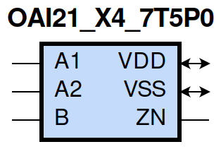
gf180mcu_fd_sc_mcu7t5v0__oai21_4 symbol
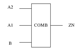
gf180mcu_fd_sc_mcu7t5v0__oai21_4 schematic

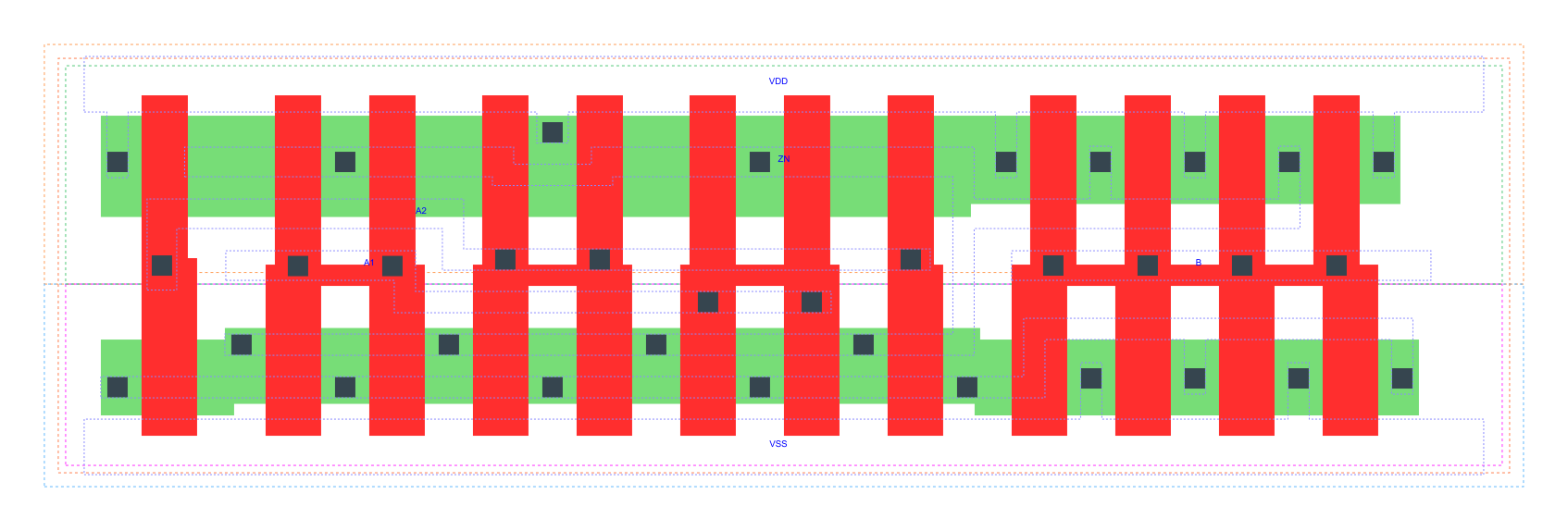
gf180mcu_fd_sc_mcu7t5v0__oai21_4 layout
OAI21_X4 is a 2-input OR into 2-input NAND, NAND[OR(A1,A2),B], 4X drive strength
Attribute |
Value |
area |
59.270400 µm2 |
Output Pin |
Function |
ZN |
(((!A1)&(!A2))|(!B)) |
A1 |
A2 |
B |
ZN |
0 |
0 |
? |
1 |
? |
? |
0 |
1 |
1 |
? |
1 |
0 |
? |
1 |
1 |
0 |
Pin |
Type |
Capacitance (pf) |
A2 |
input |
0.0184 |
A1 |
input |
0.0186 |
B |
input |
0.0165 |
Input Pin |
Output |
When Condition |
Tin (ns) |
Out Load (pf) |
Delay (ns) |
Tout (ns) |
A2(HL) |
ZN(LH) |
!A1&B |
0.0100 |
0.0010 |
0.1356 |
0.0809 |
A2(LH) |
ZN(HL) |
!A1&B |
0.0100 |
0.0010 |
0.0745 |
0.0499 |
A1(HL) |
ZN(LH) |
!A2&B |
0.0100 |
0.0010 |
0.1076 |
0.0804 |
A1(LH) |
ZN(HL) |
!A2&B |
0.0100 |
0.0010 |
0.0557 |
0.0339 |
B(LH) |
ZN(HL) |
!A1&A2 |
0.0100 |
0.0010 |
0.1000 |
0.0494 |
B(LH) |
ZN(HL) |
A1&!A2 |
0.0100 |
0.0010 |
0.0792 |
0.0346 |
B(LH) |
ZN(HL) |
A1&A2 |
0.0100 |
0.0010 |
0.0687 |
0.0335 |
B(HL) |
ZN(LH) |
!A1&A2 |
0.0100 |
0.0010 |
0.1211 |
0.1089 |
B(HL) |
ZN(LH) |
A1&!A2 |
0.0100 |
0.0010 |
0.1141 |
0.0819 |
B(HL) |
ZN(LH) |
A1&A2 |
0.0100 |
0.0010 |
0.1314 |
0.0942 |
Input Pin |
When Condition |
Tin (ns) |
Output |
Out Load (pf) |
Energy (uW/MHz) |
A1 |
!A2&B |
0.0100 |
ZN(LH) |
0.0010 |
0.4986 |
B |
!A1&A2 |
0.0100 |
ZN(HL) |
0.0010 |
0.1219 |
B |
A1&!A2 |
0.0100 |
ZN(HL) |
0.0010 |
0.0155 |
B |
A1&A2 |
0.0100 |
ZN(HL) |
0.0010 |
0.0158 |
A2 |
!A1&B |
0.0100 |
ZN(LH) |
0.0010 |
0.6067 |
A1 |
!A2&B |
0.0100 |
ZN(HL) |
0.0010 |
0.0128 |
B |
!A1&A2 |
0.0100 |
ZN(LH) |
0.0010 |
0.8996 |
B |
A1&!A2 |
0.0100 |
ZN(LH) |
0.0010 |
0.7912 |
B |
A1&A2 |
0.0100 |
ZN(LH) |
0.0010 |
0.8815 |
A2 |
!A1&B |
0.0100 |
ZN(HL) |
0.0010 |
0.1089 |
B(HL) |
!A1&!A2 |
0.0100 |
n/a |
n/a |
0.1436 |
A2(LH) |
!A1&!B |
0.0100 |
n/a |
n/a |
0.0534 |
A2(LH) |
A1&!B |
0.0100 |
n/a |
n/a |
-0.1542 |
A2(LH) |
A1&B |
0.0100 |
n/a |
n/a |
-0.1170 |
A1(LH) |
!A2&!B |
0.0100 |
n/a |
n/a |
0.0524 |
A1(LH) |
A2&!B |
0.0100 |
n/a |
n/a |
-0.1558 |
A1(LH) |
A2&B |
0.0100 |
n/a |
n/a |
-0.0404 |
A2(HL) |
!A1&!B |
0.0100 |
n/a |
n/a |
0.1590 |
A2(HL) |
A1&!B |
0.0100 |
n/a |
n/a |
0.1660 |
A2(HL) |
A1&B |
0.0100 |
n/a |
n/a |
0.1408 |
B(LH) |
!A1&!A2 |
0.0100 |
n/a |
n/a |
-0.1230 |
A1(HL) |
!A2&!B |
0.0100 |
n/a |
n/a |
0.1596 |
A1(HL) |
A2&!B |
0.0100 |
n/a |
n/a |
0.1663 |
A1(HL) |
A2&B |
0.0100 |
n/a |
n/a |
0.1111 |
When Condition |
Power (nW) |
!A1&!A2&!B |
0.2515 |
!A1&!A2&B |
0.2536 |
!A1&A2&!B |
0.4902 |
A1&!A2&!B |
0.4902 |
A1&A2&!B |
0.4914 |
!A1&A2&B |
0.4037 |
A1&!A2&B |
0.2610 |
A1&A2&B |
0.2610 |