gf180mcu_fd_sc_mcu7t5v0__nand2_4
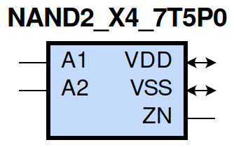
gf180mcu_fd_sc_mcu7t5v0__nand2_4 symbol
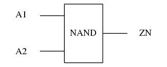
gf180mcu_fd_sc_mcu7t5v0__nand2_4 schematic

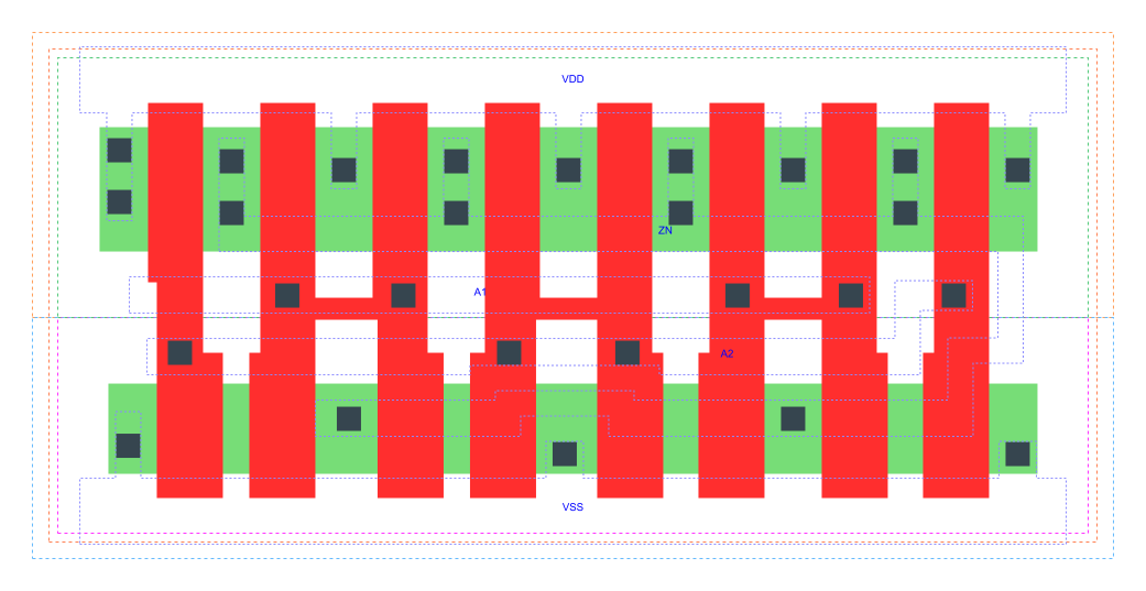
gf180mcu_fd_sc_mcu7t5v0__nand2_4 layout
NAND2_X4 is a 2-input NAND, NAND(A1,A2), 4X drive strength
Attribute |
Value |
area |
35.123200 µm2 |
Output Pin |
Function |
ZN |
((!A1)|(!A2)) |
A1 |
A2 |
ZN |
0 |
? |
1 |
? |
0 |
1 |
1 |
1 |
0 |
Pin |
Type |
Capacitance (pf) |
A1 |
input |
0.0191 |
A2 |
input |
0.0193 |
Input Pin |
Output |
When Condition |
Tin (ns) |
Out Load (pf) |
Delay (ns) |
Tout (ns) |
A1(HL) |
ZN(LH) |
A2 |
0.0100 |
0.0010 |
0.0524 |
0.0325 |
A1(LH) |
ZN(HL) |
A2 |
0.0100 |
0.0010 |
0.0505 |
0.0278 |
A2(HL) |
ZN(LH) |
A1 |
0.0100 |
0.0010 |
0.0706 |
0.0488 |
A2(LH) |
ZN(HL) |
A1 |
0.0100 |
0.0010 |
0.0616 |
0.0278 |
Input Pin |
When Condition |
Tin (ns) |
Output |
Out Load (pf) |
Energy (uW/MHz) |
A1 |
A2 |
0.0100 |
ZN(LH) |
0.0010 |
0.4191 |
A2 |
A1 |
0.0100 |
ZN(LH) |
0.0010 |
0.5676 |
A1 |
A2 |
0.0100 |
ZN(HL) |
0.0010 |
0.0076 |
A2 |
A1 |
0.0100 |
ZN(HL) |
0.0010 |
0.0078 |
A2(LH) |
!A1 |
0.0100 |
n/a |
n/a |
-0.1461 |
A1(LH) |
!A2 |
0.0100 |
n/a |
n/a |
-0.1072 |
A2(HL) |
!A1 |
0.0100 |
n/a |
n/a |
0.1629 |
A1(HL) |
!A2 |
0.0100 |
n/a |
n/a |
0.1652 |
When Condition |
Power (nW) |
!A1&!A2 |
0.1509 |
!A1&A2 |
0.1518 |
A1&!A2 |
0.3114 |
A1&A2 |
0.2615 |