gf180mcu_fd_sc_mcu7t5v0__xor2_1
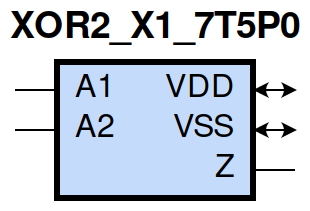
gf180mcu_fd_sc_mcu7t5v0__xor2_1 symbol
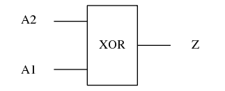
gf180mcu_fd_sc_mcu7t5v0__xor2_1 schematic

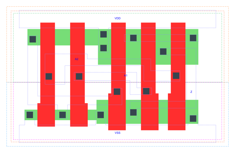
gf180mcu_fd_sc_mcu7t5v0__xor2_1 layout
XOR2_X1 is a 2-input exclusive OR, 1X drive strength
Attribute |
Value |
area |
26.342400 µm2 |
Output Pin |
Function |
Z |
(A1^A2) |
A1 |
A2 |
Z |
1 |
0 |
1 |
0 |
1 |
1 |
1 |
1 |
0 |
0 |
0 |
0 |
Pin |
Type |
Capacitance (pf) |
A2 |
input |
0.0075 |
A1 |
input |
0.0075 |
Input Pin |
Output |
When Condition |
Tin (ns) |
Out Load (pf) |
Delay (ns) |
Tout (ns) |
A2(HL) |
Z(HL) |
!A1 |
0.0100 |
0.0010 |
0.3753 |
0.0902 |
A2(LH) |
Z(LH) |
!A1 |
0.0100 |
0.0010 |
0.2481 |
0.0905 |
A2(HL) |
Z(LH) |
A1 |
0.0100 |
0.0010 |
0.1369 |
0.1151 |
A2(LH) |
Z(HL) |
A1 |
0.0100 |
0.0010 |
0.0769 |
0.0389 |
A1(LH) |
Z(HL) |
A2 |
0.0100 |
0.0010 |
0.0655 |
0.0389 |
A1(HL) |
Z(LH) |
A2 |
0.0100 |
0.0010 |
0.1055 |
0.0847 |
A1(LH) |
Z(LH) |
!A2 |
0.0100 |
0.0010 |
0.3016 |
0.1182 |
A1(HL) |
Z(HL) |
!A2 |
0.0100 |
0.0010 |
0.4031 |
0.0897 |
Input Pin |
When Condition |
Tin (ns) |
Output |
Out Load (pf) |
Energy (uW/MHz) |
A2 |
!A1 |
0.0100 |
Z(HL) |
0.0010 |
0.2922 |
A2 |
A1 |
0.0100 |
Z(HL) |
0.0010 |
-0.0010 |
A1 |
A2 |
0.0100 |
Z(HL) |
0.0010 |
-0.0109 |
A1 |
!A2 |
0.0100 |
Z(HL) |
0.0010 |
0.3092 |
A2 |
!A1 |
0.0100 |
Z(LH) |
0.0010 |
0.1582 |
A2 |
A1 |
0.0100 |
Z(LH) |
0.0010 |
0.1766 |
A1 |
A2 |
0.0100 |
Z(LH) |
0.0010 |
0.1445 |
A1 |
!A2 |
0.0100 |
Z(LH) |
0.0010 |
0.2110 |
When Condition |
Power (nW) |
!A1&!A2 |
0.2104 |
A1&A2 |
0.1291 |
!A1&A2 |
0.1270 |
A1&!A2 |
0.2029 |