gf180mcu_fd_sc_mcu7t5v0__dffnsnq_1
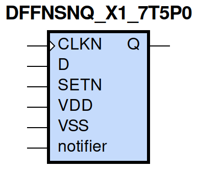
gf180mcu_fd_sc_mcu7t5v0__dffnsnq_1 symbol
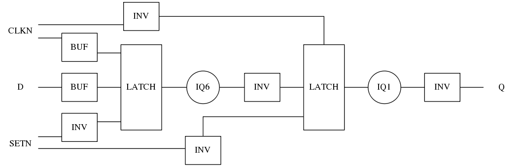
gf180mcu_fd_sc_mcu7t5v0__dffnsnq_1 schematic

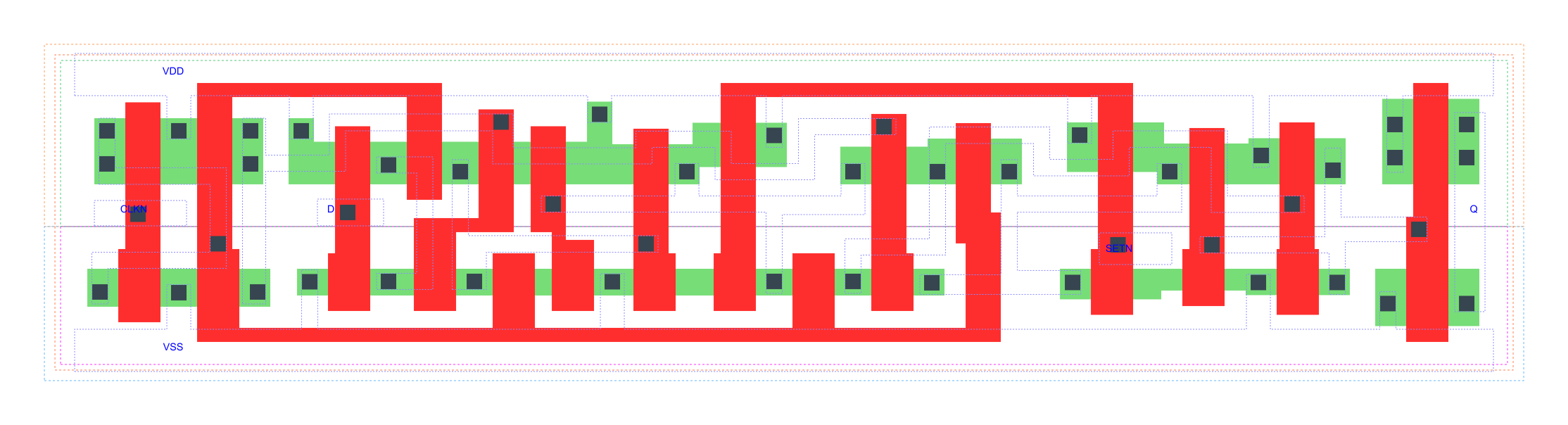
gf180mcu_fd_sc_mcu7t5v0__dffnsnq_1 layout
DFFNSNQ_X1 is a negative edge triggered D-type flip flop, active low set and 1X drive strength
Attribute |
Value |
area |
79.027200 µm2 |
TRUTH TABLE
Input |
Output |
||
SETN |
D |
CLKN |
Q |
H |
L |
↓ |
L |
H |
H |
↓ |
H |
L |
X |
X |
H |
Constraint Pin |
Related Pin |
setup(ns) |
hold(ns) |
D(HL) |
CLKN(HL) |
0.3150 |
0.0060 |
D(LH) |
CLKN(HL) |
0.2180 |
0.1320 |
Constraint Pin |
Related Pin |
recovery(ns) |
removal(ns) |
SETN(LH) |
CLKN(HL) |
0.0970 |
0.1140 |
Constraint Pin |
Related Pin |
Minimum Pulse Width(ns) |
CLKN(LHL) |
CLKN(LH) |
0.4550 |
CLKN(LHL) |
CLKN(LH) |
0.4120 |
CLKN(HLH) |
CLKN(HL) |
0.4370 |
CLKN(HLH) |
CLKN(HL) |
0.4270 |
SETN(HLH) |
SETN(HL) |
0.3680 |
SETN(HLH) |
SETN(HL) |
0.3390 |
SETN(HLH) |
SETN(HL) |
0.3680 |
SETN(HLH) |
SETN(HL) |
0.3390 |
Pin |
Type |
Capacitance (pf) |
CLKN |
input |
0.0038 |
D |
input |
0.0026 |
SETN |
input |
0.0064 |
Input Pin |
Output |
When Condition |
Tin (ns) |
Out Load (pf) |
Delay (ns) |
Tout (ns) |
CLKN(HL) |
Q(LH) |
D&SETN |
0.0100 |
0.0010 |
0.6557 |
0.0465 |
CLKN(HL) |
Q(HL) |
!D&SETN |
0.0100 |
0.0010 |
0.6131 |
0.0459 |
SETN(HL) |
Q(LH) |
!CLKN&!D |
0.0100 |
0.0010 |
0.5421 |
0.0457 |
SETN(HL) |
Q(LH) |
CLKN&!D |
0.0100 |
0.0010 |
0.4810 |
0.0451 |
SETN(HL) |
Q(LH) |
!CLKN&D |
0.0100 |
0.0010 |
0.5418 |
0.0456 |
SETN(HL) |
Q(LH) |
CLKN&D |
0.0100 |
0.0010 |
0.4814 |
0.0450 |
Input Pin |
When Condition |
Tin (ns) |
Output |
Out Load (pf) |
Energy (uW/MHz) |
SETN |
!CLKN&!D |
0.0100 |
Q(LH) |
0.0010 |
0.5913 |
SETN |
CLKN&!D |
0.0100 |
Q(LH) |
0.0010 |
0.5101 |
SETN |
!CLKN&D |
0.0100 |
Q(LH) |
0.0010 |
0.5911 |
SETN |
CLKN&D |
0.0100 |
Q(LH) |
0.0010 |
0.4137 |
CLKN |
D&SETN |
0.0100 |
Q(LH) |
0.0010 |
0.7602 |
CLKN |
!D&SETN |
0.0100 |
Q(HL) |
0.0010 |
0.6526 |
SETN(HL) |
!CLKN&!D |
0.0100 |
n/a |
n/a |
0.0473 |
SETN(HL) |
CLKN&!D |
0.0100 |
n/a |
n/a |
0.1425 |
SETN(HL) |
!CLKN&D |
0.0100 |
n/a |
n/a |
0.0473 |
SETN(HL) |
CLKN&D |
0.0100 |
n/a |
n/a |
0.0472 |
CLKN(LH) |
!D&!SETN |
0.0100 |
n/a |
n/a |
0.3092 |
CLKN(LH) |
D&!SETN |
0.0100 |
n/a |
n/a |
0.2258 |
CLKN(LH) |
!D&SETN |
0.0100 |
n/a |
n/a |
0.2238 |
CLKN(LH) |
D&SETN |
0.0100 |
n/a |
n/a |
0.2255 |
CLKN(HL) |
!D&!SETN |
0.0100 |
n/a |
n/a |
0.3753 |
CLKN(HL) |
D&!SETN |
0.0100 |
n/a |
n/a |
0.3241 |
CLKN(HL) |
!D&SETN |
0.0100 |
n/a |
n/a |
0.3190 |
CLKN(HL) |
D&SETN |
0.0100 |
n/a |
n/a |
0.3240 |
D(HL) |
!CLKN&!SETN |
0.0100 |
n/a |
n/a |
0.0609 |
D(HL) |
CLKN&!SETN |
0.0100 |
n/a |
n/a |
0.1478 |
D(HL) |
!CLKN&SETN |
0.0100 |
n/a |
n/a |
0.0610 |
D(HL) |
CLKN&SETN |
0.0100 |
n/a |
n/a |
0.2183 |
D(LH) |
!CLKN&!SETN |
0.0100 |
n/a |
n/a |
0.0053 |
D(LH) |
CLKN&!SETN |
0.0100 |
n/a |
n/a |
0.0538 |
D(LH) |
!CLKN&SETN |
0.0100 |
n/a |
n/a |
0.0053 |
D(LH) |
CLKN&SETN |
0.0100 |
n/a |
n/a |
0.1750 |
SETN(LH) |
!CLKN&!D |
0.0100 |
n/a |
n/a |
-0.0251 |
SETN(LH) |
!CLKN&D |
0.0100 |
n/a |
n/a |
-0.0251 |
SETN(LH) |
CLKN&!D |
0.0100 |
n/a |
n/a |
0.0304 |
SETN(LH) |
CLKN&D |
0.0100 |
n/a |
n/a |
-0.0252 |
When Condition |
Power (nW) |
!CLKN&!D&!SETN |
0.4463 |
!CLKN&D&!SETN |
0.4449 |
CLKN&!D&!SETN |
0.4094 |
CLKN&D&!SETN |
0.4067 |
!CLKN&!D&SETN |
0.5307 |
CLKN&!D&SETN |
0.6143 |
CLKN&D&SETN |
0.6042 |
!CLKN&D&SETN |
0.6383 |