gf180mcu_fd_sc_mcu7t5v0__xnor2_1
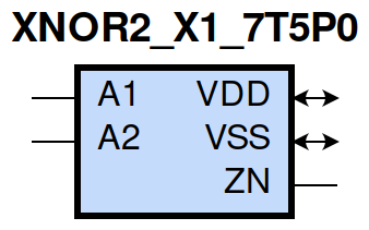
gf180mcu_fd_sc_mcu7t5v0__xnor2_1 symbol
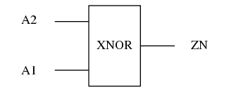
gf180mcu_fd_sc_mcu7t5v0__xnor2_1 schematic

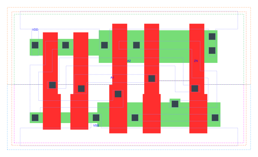
gf180mcu_fd_sc_mcu7t5v0__xnor2_1 layout
XNOR2_X1 is a 2-input exclusive NOR, 1X drive strength
Attribute |
Value |
area |
28.537600 µm2 |
Output Pin |
Function |
ZN |
(!(A1^A2)) |
A1 |
A2 |
ZN |
1 |
1 |
1 |
0 |
0 |
1 |
1 |
0 |
0 |
0 |
1 |
0 |
Pin |
Type |
Capacitance (pf) |
A2 |
input |
0.0074 |
A1 |
input |
0.0071 |
Input Pin |
Output |
When Condition |
Tin (ns) |
Out Load (pf) |
Delay (ns) |
Tout (ns) |
A2(LH) |
ZN(LH) |
A1 |
0.0100 |
0.0010 |
0.3108 |
0.1043 |
A2(HL) |
ZN(LH) |
!A1 |
0.0100 |
0.0010 |
0.1660 |
0.1039 |
A2(HL) |
ZN(HL) |
A1 |
0.0100 |
0.0010 |
0.2474 |
0.0585 |
A2(LH) |
ZN(HL) |
!A1 |
0.0100 |
0.0010 |
0.0880 |
0.0613 |
A1(HL) |
ZN(LH) |
!A2 |
0.0100 |
0.0010 |
0.1346 |
0.1035 |
A1(HL) |
ZN(HL) |
A2 |
0.0100 |
0.0010 |
0.2881 |
0.0741 |
A1(LH) |
ZN(HL) |
!A2 |
0.0100 |
0.0010 |
0.0671 |
0.0434 |
A1(LH) |
ZN(LH) |
A2 |
0.0100 |
0.0010 |
0.3229 |
0.1044 |
Input Pin |
When Condition |
Tin (ns) |
Output |
Out Load (pf) |
Energy (uW/MHz) |
A2 |
A1 |
0.0100 |
ZN(LH) |
0.0010 |
0.2153 |
A2 |
!A1 |
0.0100 |
ZN(LH) |
0.0010 |
0.1822 |
A1 |
!A2 |
0.0100 |
ZN(LH) |
0.0010 |
0.1549 |
A1 |
A2 |
0.0100 |
ZN(LH) |
0.0010 |
0.2376 |
A1 |
A2 |
0.0100 |
ZN(HL) |
0.0010 |
0.2626 |
A1 |
!A2 |
0.0100 |
ZN(HL) |
0.0010 |
-0.0078 |
A2 |
A1 |
0.0100 |
ZN(HL) |
0.0010 |
0.2203 |
A2 |
!A1 |
0.0100 |
ZN(HL) |
0.0010 |
0.0261 |
When Condition |
Power (nW) |
!A1&!A2 |
0.1265 |
A1&A2 |
0.2127 |
!A1&A2 |
0.2063 |
A1&!A2 |
0.1304 |