gf180mcu_fd_sc_mcu7t5v0__and2_1
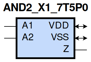
gf180mcu_fd_sc_mcu7t5v0__and2_1 symbol
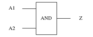
gf180mcu_fd_sc_mcu7t5v0__and2_1 schematic

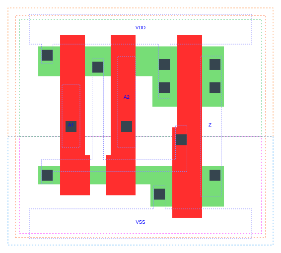
gf180mcu_fd_sc_mcu7t5v0__and2_1 layout
AND2_X1 is a 2-input AND, AND(A1,A2), 1X drive strength
Attribute |
Value |
area |
17.561600 µm2 |
Output Pin |
Function |
Z |
(A1&A2) |
A1 |
A2 |
Z |
1 |
1 |
1 |
0 |
? |
0 |
? |
0 |
0 |
Pin |
Type |
Capacitance (pf) |
A1 |
input |
0.0028 |
A2 |
input |
0.0028 |
Input Pin |
Output |
When Condition |
Tin (ns) |
Out Load (pf) |
Delay (ns) |
Tout (ns) |
A1(LH) |
Z(LH) |
A2 |
0.0100 |
0.0010 |
0.2235 |
0.0480 |
A1(HL) |
Z(HL) |
A2 |
0.0100 |
0.0010 |
0.1877 |
0.0391 |
A2(HL) |
Z(HL) |
A1 |
0.0100 |
0.0010 |
0.2029 |
0.0418 |
A2(LH) |
Z(LH) |
A1 |
0.0100 |
0.0010 |
0.2347 |
0.0481 |
Input Pin |
When Condition |
Tin (ns) |
Output |
Out Load (pf) |
Energy (uW/MHz) |
A2 |
A1 |
0.0100 |
Z(HL) |
0.0010 |
0.2101 |
A2 |
A1 |
0.0100 |
Z(LH) |
0.0010 |
0.1181 |
A1 |
A2 |
0.0100 |
Z(LH) |
0.0010 |
0.1179 |
A1 |
A2 |
0.0100 |
Z(HL) |
0.0010 |
0.1893 |
A2(LH) |
!A1 |
0.0100 |
n/a |
n/a |
-0.0192 |
A1(LH) |
!A2 |
0.0100 |
n/a |
n/a |
-0.0136 |
A1(HL) |
!A2 |
0.0100 |
n/a |
n/a |
0.0214 |
A2(HL) |
!A1 |
0.0100 |
n/a |
n/a |
0.0213 |
When Condition |
Power (nW) |
!A1&!A2 |
0.1021 |
!A1&A2 |
0.1038 |
A1&!A2 |
0.1443 |
A1&A2 |
0.1277 |