gf180mcu_fd_sc_mcu7t5v0__nor2_4
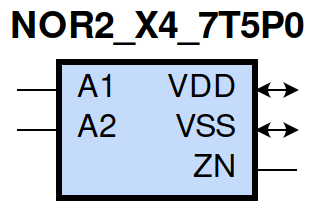
gf180mcu_fd_sc_mcu7t5v0__nor2_4 symbol
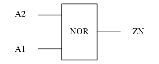
gf180mcu_fd_sc_mcu7t5v0__nor2_4 schematic

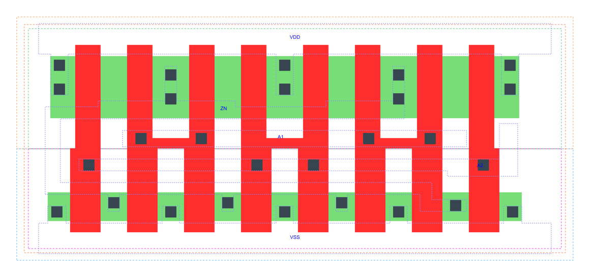
gf180mcu_fd_sc_mcu7t5v0__nor2_4 layout
NOR2_X4 is a 2-input NOR, NOR(A1,A2), 4X drive strength
Attribute |
Value |
area |
39.513600 µm2 |
Output Pin |
Function |
ZN |
((!A1)&(!A2)) |
A1 |
A2 |
ZN |
0 |
0 |
1 |
1 |
? |
0 |
? |
1 |
0 |
Pin |
Type |
Capacitance (pf) |
A2 |
input |
0.0176 |
A1 |
input |
0.0177 |
Input Pin |
Output |
When Condition |
Tin (ns) |
Out Load (pf) |
Delay (ns) |
Tout (ns) |
A2(HL) |
ZN(LH) |
!A1 |
0.0100 |
0.0010 |
0.0975 |
0.0585 |
A2(LH) |
ZN(HL) |
!A1 |
0.0100 |
0.0010 |
0.0636 |
0.0361 |
A1(HL) |
ZN(LH) |
!A2 |
0.0100 |
0.0010 |
0.0732 |
0.0574 |
A1(LH) |
ZN(HL) |
!A2 |
0.0100 |
0.0010 |
0.0459 |
0.0222 |
Input Pin |
When Condition |
Tin (ns) |
Output |
Out Load (pf) |
Energy (uW/MHz) |
A1 |
!A2 |
0.0100 |
ZN(LH) |
0.0010 |
0.4119 |
A2 |
!A1 |
0.0100 |
ZN(LH) |
0.0010 |
0.5327 |
A1 |
!A2 |
0.0100 |
ZN(HL) |
0.0010 |
-0.0245 |
A2 |
!A1 |
0.0100 |
ZN(HL) |
0.0010 |
0.0658 |
A2(LH) |
A1 |
0.0100 |
n/a |
n/a |
-0.1313 |
A1(LH) |
A2 |
0.0100 |
n/a |
n/a |
-0.0444 |
A2(HL) |
A1 |
0.0100 |
n/a |
n/a |
0.1571 |
A1(HL) |
A2 |
0.0100 |
n/a |
n/a |
0.1055 |
When Condition |
Power (nW) |
!A1&!A2 |
0.2540 |
!A1&A2 |
0.2985 |
A1&!A2 |
0.1560 |
A1&A2 |
0.1560 |