gf180mcu_fd_sc_mcu7t5v0__nand3_2
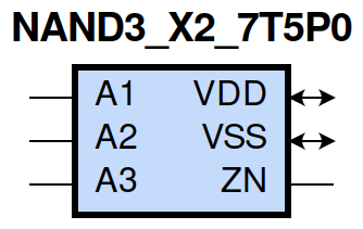
gf180mcu_fd_sc_mcu7t5v0__nand3_2 symbol
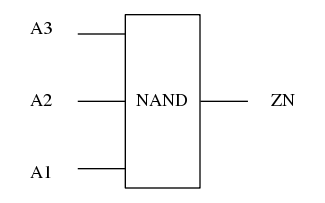
gf180mcu_fd_sc_mcu7t5v0__nand3_2 schematic

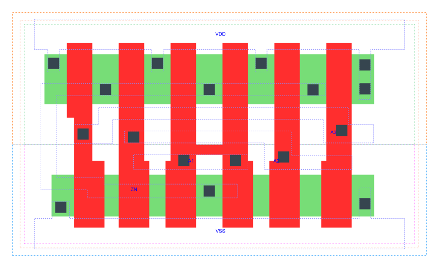
gf180mcu_fd_sc_mcu7t5v0__nand3_2 layout
NAND3_X2 is a 3-input NAND, NAND(A1,A2,A3), 2X drive strength
Attribute |
Value |
area |
28.537600 µm2 |
Output Pin |
Function |
ZN |
((!A1)|(!A2)|(!A3)) |
A1 |
A2 |
A3 |
ZN |
0 |
? |
? |
1 |
? |
0 |
? |
1 |
? |
? |
0 |
1 |
1 |
1 |
1 |
0 |
Pin |
Type |
Capacitance (pf) |
A3 |
input |
0.0097 |
A2 |
input |
0.0093 |
A1 |
input |
0.0087 |
Input Pin |
Output |
When Condition |
Tin (ns) |
Out Load (pf) |
Delay (ns) |
Tout (ns) |
A3(LH) |
ZN(HL) |
A1&A2 |
0.0100 |
0.0010 |
0.1010 |
0.0486 |
A3(HL) |
ZN(LH) |
A1&A2 |
0.0100 |
0.0010 |
0.1096 |
0.0814 |
A2(HL) |
ZN(LH) |
A1&A3 |
0.0100 |
0.0010 |
0.0932 |
0.0644 |
A2(LH) |
ZN(HL) |
A1&A3 |
0.0100 |
0.0010 |
0.0900 |
0.0484 |
A1(HL) |
ZN(LH) |
A2&A3 |
0.0100 |
0.0010 |
0.0694 |
0.0452 |
A1(LH) |
ZN(HL) |
A2&A3 |
0.0100 |
0.0010 |
0.0700 |
0.0482 |
Input Pin |
When Condition |
Tin (ns) |
Output |
Out Load (pf) |
Energy (uW/MHz) |
A1 |
A2&A3 |
0.0100 |
ZN(LH) |
0.0010 |
0.2167 |
A2 |
A1&A3 |
0.0100 |
ZN(LH) |
0.0010 |
0.2966 |
A3 |
A1&A2 |
0.0100 |
ZN(HL) |
0.0010 |
0.0265 |
A1 |
A2&A3 |
0.0100 |
ZN(HL) |
0.0010 |
0.0264 |
A2 |
A1&A3 |
0.0100 |
ZN(HL) |
0.0010 |
0.0265 |
A3 |
A1&A2 |
0.0100 |
ZN(LH) |
0.0010 |
0.3697 |
A3(LH) |
!A1&!A2 |
0.0100 |
n/a |
n/a |
-0.0637 |
A3(LH) |
!A1&A2 |
0.0100 |
n/a |
n/a |
-0.0635 |
A3(LH) |
A1&!A2 |
0.0100 |
n/a |
n/a |
-0.0636 |
A2(LH) |
!A1&!A3 |
0.0100 |
n/a |
n/a |
-0.0639 |
A2(LH) |
!A1&A3 |
0.0100 |
n/a |
n/a |
-0.0635 |
A2(LH) |
A1&!A3 |
0.0100 |
n/a |
n/a |
-0.0459 |
A1(LH) |
!A2&!A3 |
0.0100 |
n/a |
n/a |
-0.0428 |
A1(LH) |
!A2&A3 |
0.0100 |
n/a |
n/a |
-0.0428 |
A1(LH) |
A2&!A3 |
0.0100 |
n/a |
n/a |
0.0386 |
A3(HL) |
!A1&!A2 |
0.0100 |
n/a |
n/a |
0.0637 |
A3(HL) |
!A1&A2 |
0.0100 |
n/a |
n/a |
0.0709 |
A3(HL) |
A1&!A2 |
0.0100 |
n/a |
n/a |
0.0691 |
A2(HL) |
!A1&!A3 |
0.0100 |
n/a |
n/a |
0.0884 |
A2(HL) |
!A1&A3 |
0.0100 |
n/a |
n/a |
0.0774 |
A2(HL) |
A1&!A3 |
0.0100 |
n/a |
n/a |
0.0718 |
A1(HL) |
!A2&!A3 |
0.0100 |
n/a |
n/a |
0.0733 |
A1(HL) |
!A2&A3 |
0.0100 |
n/a |
n/a |
0.0732 |
A1(HL) |
A2&!A3 |
0.0100 |
n/a |
n/a |
0.0724 |
When Condition |
Power (nW) |
!A1&!A2&!A3 |
0.1004 |
!A1&!A2&A3 |
0.1004 |
!A1&A2&!A3 |
0.1006 |
!A1&A2&A3 |
0.1009 |
A1&!A2&!A3 |
0.1804 |
A1&!A2&A3 |
0.1807 |
A1&A2&!A3 |
0.2590 |
A1&A2&A3 |
0.2081 |