gf180mcu_fd_sc_mcu7t5v0__xor3_4
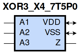
gf180mcu_fd_sc_mcu7t5v0__xor3_4 symbol
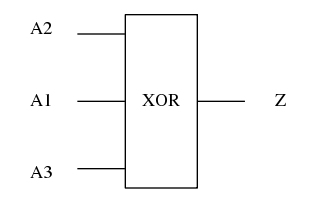
gf180mcu_fd_sc_mcu7t5v0__xor3_4 schematic

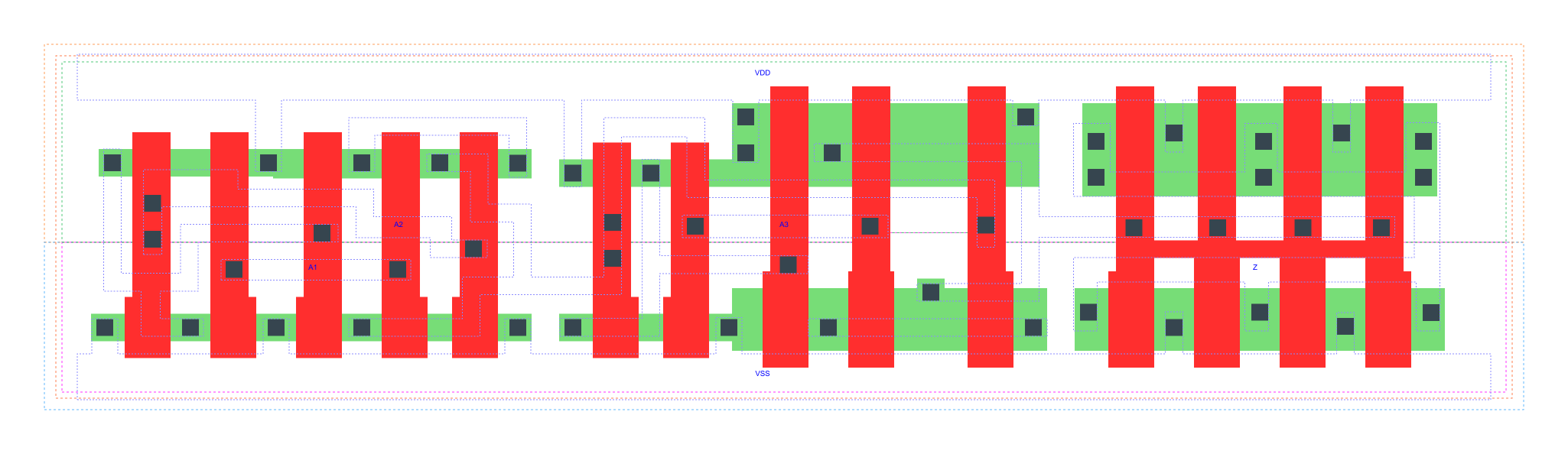
gf180mcu_fd_sc_mcu7t5v0__xor3_4 layout
XOR3_X4 is a 3-input exclusive OR, 4X drive strength
Attribute |
Value |
area |
72.441600 µm2 |
Output Pin |
Function |
Z |
(A1^A2^A3) |
A1 |
A2 |
A3 |
Z |
1 |
1 |
1 |
1 |
1 |
0 |
0 |
1 |
0 |
1 |
0 |
1 |
0 |
0 |
1 |
1 |
1 |
1 |
0 |
0 |
1 |
0 |
1 |
0 |
0 |
1 |
1 |
0 |
0 |
0 |
0 |
0 |
Pin |
Type |
Capacitance (pf) |
A2 |
input |
0.0049 |
A1 |
input |
0.0046 |
A3 |
input |
0.0068 |
Input Pin |
Output |
When Condition |
Tin (ns) |
Out Load (pf) |
Delay (ns) |
Tout (ns) |
A2(HL) |
Z(HL) |
!A1&!A3 |
0.0100 |
0.0010 |
0.9860 |
0.0769 |
A2(HL) |
Z(HL) |
A1&A3 |
0.0100 |
0.0010 |
1.1225 |
0.0573 |
A2(LH) |
Z(LH) |
!A1&!A3 |
0.0100 |
0.0010 |
1.1069 |
0.0603 |
A2(LH) |
Z(LH) |
A1&A3 |
0.0100 |
0.0010 |
0.8180 |
0.0525 |
A2(HL) |
Z(LH) |
!A1&A3 |
0.0100 |
0.0010 |
1.0978 |
0.0527 |
A2(HL) |
Z(LH) |
A1&!A3 |
0.0100 |
0.0010 |
1.0096 |
0.0607 |
A2(LH) |
Z(HL) |
!A1&A3 |
0.0100 |
0.0010 |
1.2259 |
0.0572 |
A2(LH) |
Z(HL) |
A1&!A3 |
0.0100 |
0.0010 |
0.7040 |
0.0771 |
A1(LH) |
Z(HL) |
!A2&A3 |
0.0100 |
0.0010 |
1.2773 |
0.0573 |
A1(LH) |
Z(HL) |
A2&!A3 |
0.0100 |
0.0010 |
0.6928 |
0.0772 |
A1(HL) |
Z(LH) |
!A2&A3 |
0.0100 |
0.0010 |
1.1269 |
0.0524 |
A1(HL) |
Z(LH) |
A2&!A3 |
0.0100 |
0.0010 |
0.9613 |
0.0600 |
A1(LH) |
Z(LH) |
!A2&!A3 |
0.0100 |
0.0010 |
1.1641 |
0.0607 |
A1(LH) |
Z(LH) |
A2&A3 |
0.0100 |
0.0010 |
0.8069 |
0.0525 |
A1(HL) |
Z(HL) |
!A2&!A3 |
0.0100 |
0.0010 |
1.0153 |
0.0766 |
A1(HL) |
Z(HL) |
A2&A3 |
0.0100 |
0.0010 |
1.0805 |
0.0572 |
A3(LH) |
Z(LH) |
!A1&!A2 |
0.0100 |
0.0010 |
0.2935 |
0.0514 |
A3(LH) |
Z(LH) |
A1&A2 |
0.0100 |
0.0010 |
0.2935 |
0.0514 |
A3(HL) |
Z(LH) |
!A1&A2 |
0.0100 |
0.0010 |
0.6084 |
0.0548 |
A3(HL) |
Z(LH) |
A1&!A2 |
0.0100 |
0.0010 |
0.6084 |
0.0548 |
A3(HL) |
Z(HL) |
!A1&!A2 |
0.0100 |
0.0010 |
0.4416 |
0.0765 |
A3(HL) |
Z(HL) |
A1&A2 |
0.0100 |
0.0010 |
0.4414 |
0.0767 |
A3(LH) |
Z(HL) |
!A1&A2 |
0.0100 |
0.0010 |
0.5011 |
0.0574 |
A3(LH) |
Z(HL) |
A1&!A2 |
0.0100 |
0.0010 |
0.5011 |
0.0574 |
Input Pin |
When Condition |
Tin (ns) |
Output |
Out Load (pf) |
Energy (uW/MHz) |
A3 |
!A1&!A2 |
0.0100 |
Z(LH) |
0.0010 |
0.5632 |
A3 |
A1&A2 |
0.0100 |
Z(LH) |
0.0010 |
0.5624 |
A3 |
!A1&A2 |
0.0100 |
Z(LH) |
0.0010 |
0.8796 |
A3 |
A1&!A2 |
0.0100 |
Z(LH) |
0.0010 |
0.8796 |
A2 |
!A1&!A3 |
0.0100 |
Z(HL) |
0.0010 |
1.2010 |
A2 |
A1&A3 |
0.0100 |
Z(HL) |
0.0010 |
1.1647 |
A2 |
!A1&A3 |
0.0100 |
Z(HL) |
0.0010 |
1.1566 |
A2 |
A1&!A3 |
0.0100 |
Z(HL) |
0.0010 |
1.0490 |
A1 |
!A2&A3 |
0.0100 |
Z(HL) |
0.0010 |
1.1869 |
A1 |
A2&!A3 |
0.0100 |
Z(HL) |
0.0010 |
1.0422 |
A1 |
!A2&!A3 |
0.0100 |
Z(HL) |
0.0010 |
1.2113 |
A1 |
A2&A3 |
0.0100 |
Z(HL) |
0.0010 |
1.1447 |
A2 |
!A1&!A3 |
0.0100 |
Z(LH) |
0.0010 |
1.0588 |
A2 |
A1&A3 |
0.0100 |
Z(LH) |
0.0010 |
0.8013 |
A2 |
!A1&A3 |
0.0100 |
Z(LH) |
0.0010 |
0.9576 |
A2 |
A1&!A3 |
0.0100 |
Z(LH) |
0.0010 |
1.0823 |
A1 |
!A2&A3 |
0.0100 |
Z(LH) |
0.0010 |
0.9684 |
A1 |
A2&!A3 |
0.0100 |
Z(LH) |
0.0010 |
1.0460 |
A1 |
!A2&!A3 |
0.0100 |
Z(LH) |
0.0010 |
1.1039 |
A1 |
A2&A3 |
0.0100 |
Z(LH) |
0.0010 |
0.7948 |
A3 |
!A1&!A2 |
0.0100 |
Z(HL) |
0.0010 |
1.0136 |
A3 |
A1&A2 |
0.0100 |
Z(HL) |
0.0010 |
1.0137 |
A3 |
!A1&A2 |
0.0100 |
Z(HL) |
0.0010 |
0.8828 |
A3 |
A1&!A2 |
0.0100 |
Z(HL) |
0.0010 |
0.8828 |
When Condition |
Power (nW) |
!A1&!A2&!A3 |
0.3932 |
!A1&A2&A3 |
0.3995 |
A1&!A2&A3 |
0.4759 |
A1&A2&!A3 |
0.3104 |
!A1&!A2&A3 |
0.3929 |
!A1&A2&!A3 |
0.3892 |
A1&!A2&!A3 |
0.4657 |
A1&A2&A3 |
0.3101 |