gf180mcu_fd_sc_mcu7t5v0__nor2_2
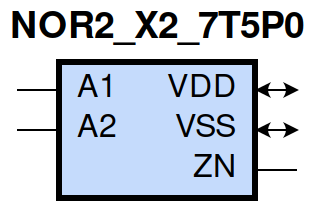
gf180mcu_fd_sc_mcu7t5v0__nor2_2 symbol
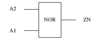
gf180mcu_fd_sc_mcu7t5v0__nor2_2 schematic

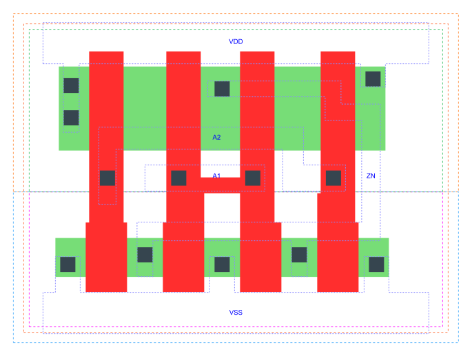
gf180mcu_fd_sc_mcu7t5v0__nor2_2 layout
NOR2_X2 is a 2-input NOR, NOR(A1,A2), 2X drive strength
Attribute |
Value |
area |
21.952000 µm2 |
Output Pin |
Function |
ZN |
((!A1)&(!A2)) |
A1 |
A2 |
ZN |
0 |
0 |
1 |
1 |
? |
0 |
? |
1 |
0 |
Pin |
Type |
Capacitance (pf) |
A2 |
input |
0.0086 |
A1 |
input |
0.0083 |
Input Pin |
Output |
When Condition |
Tin (ns) |
Out Load (pf) |
Delay (ns) |
Tout (ns) |
A2(HL) |
ZN(LH) |
!A1 |
0.0100 |
0.0010 |
0.0990 |
0.0588 |
A2(LH) |
ZN(HL) |
!A1 |
0.0100 |
0.0010 |
0.0642 |
0.0366 |
A1(HL) |
ZN(LH) |
!A2 |
0.0100 |
0.0010 |
0.0728 |
0.0575 |
A1(LH) |
ZN(HL) |
!A2 |
0.0100 |
0.0010 |
0.0457 |
0.0222 |
Input Pin |
When Condition |
Tin (ns) |
Output |
Out Load (pf) |
Energy (uW/MHz) |
A1 |
!A2 |
0.0100 |
ZN(LH) |
0.0010 |
0.1974 |
A2 |
!A1 |
0.0100 |
ZN(LH) |
0.0010 |
0.2582 |
A1 |
!A2 |
0.0100 |
ZN(HL) |
0.0010 |
-0.0163 |
A2 |
!A1 |
0.0100 |
ZN(HL) |
0.0010 |
0.0339 |
A2(LH) |
A1 |
0.0100 |
n/a |
n/a |
-0.0654 |
A1(LH) |
A2 |
0.0100 |
n/a |
n/a |
-0.0224 |
A2(HL) |
A1 |
0.0100 |
n/a |
n/a |
0.0786 |
A1(HL) |
A2 |
0.0100 |
n/a |
n/a |
0.0573 |
When Condition |
Power (nW) |
!A1&!A2 |
0.1520 |
!A1&A2 |
0.1743 |
A1&!A2 |
0.1030 |
A1&A2 |
0.1030 |