gf180mcu_fd_sc_mcu7t5v0__invz_x12
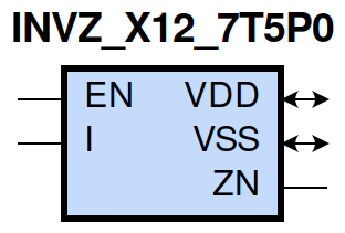
gf180mcu_fd_sc_mcu7t5v0__invz_x12 symbol
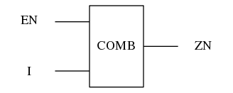
gf180mcu_fd_sc_mcu7t5v0__invz_x12 schematic

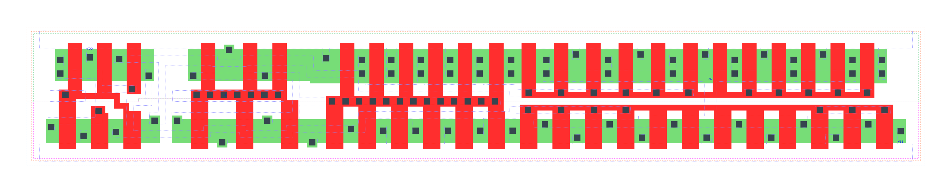
gf180mcu_fd_sc_mcu7t5v0__invz_x12 layout
INVZ_X12 is a tri-state inverter, 12X drive strength
Attribute |
Value |
area |
118.540800 µm2 |
Output Pin |
Function |
ZN |
(!I) |
EN |
I |
ZN |
1 |
0 |
1 |
1 |
1 |
0 |
0 |
? |
z |
Pin |
Type |
Capacitance (pf) |
EN |
input |
0.0090 |
I |
input |
0.0137 |
Input Pin |
Output |
When Condition |
Tin (ns) |
Out Load (pf) |
Delay (ns) |
Tout (ns) |
EN(LH) |
ZN(ZL) |
I |
0.0100 |
0.0010 |
0.1855 |
0.0460 |
EN(LH) |
ZN(ZH) |
!I |
0.0100 |
0.0010 |
0.2232 |
0.0555 |
EN(HL) |
ZN(HZ) |
!I |
0.0100 |
0.5190 |
0.0000 |
|
EN(HL) |
ZN(LZ) |
I |
0.0100 |
0.3910 |
0.0000 |
|
I(LH) |
ZN(HL) |
EN |
0.0100 |
0.0010 |
0.3249 |
0.0446 |
I(HL) |
ZN(LH) |
EN |
0.0100 |
0.0010 |
0.4067 |
0.0531 |
Input Pin |
When Condition |
Tin (ns) |
Output |
Out Load (pf) |
Energy (uW/MHz) |
I |
EN |
0.0100 |
ZN(HL) |
0.0010 |
1.8073 |
I |
EN |
0.0100 |
ZN(LH) |
0.0010 |
1.7887 |
EN |
I |
0.0100 |
ZN(HL) |
0.0010 |
1.0784 |
EN(HL) |
I |
0.0100 |
n/a |
n/a |
0.2443 |
EN(HL) |
!I |
0.0100 |
n/a |
n/a |
0.5934 |
EN |
!I |
0.0100 |
ZN(LH) |
0.0010 |
0.9881 |
I(LH) |
!EN |
0.0100 |
n/a |
n/a |
0.2119 |
I(HL) |
!EN |
0.0100 |
n/a |
n/a |
0.6242 |
When Condition |
Power (nW) |
!EN&!I |
0.3590 |
!EN&I |
0.3619 |
EN&!I |
0.6934 |
EN&I |
0.7014 |