gf180mcu_fd_sc_mcu7t5v0__and2_4
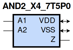
gf180mcu_fd_sc_mcu7t5v0__and2_4 symbol
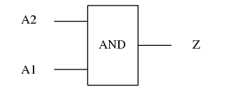
gf180mcu_fd_sc_mcu7t5v0__and2_4 schematic

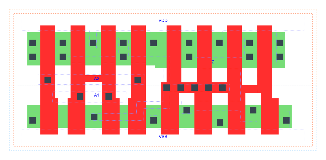
gf180mcu_fd_sc_mcu7t5v0__and2_4 layout
AND2_X4 is a 2-input AND, AND(A1,A2), 4X drive strength
Attribute |
Value |
area |
37.318400 µm2 |
Output Pin |
Function |
Z |
(A1&A2) |
A1 |
A2 |
Z |
1 |
1 |
1 |
0 |
? |
0 |
? |
0 |
0 |
Pin |
Type |
Capacitance (pf) |
A2 |
input |
0.0093 |
A1 |
input |
0.0089 |
Input Pin |
Output |
When Condition |
Tin (ns) |
Out Load (pf) |
Delay (ns) |
Tout (ns) |
A2(HL) |
Z(HL) |
A1 |
0.0100 |
0.0010 |
0.1754 |
0.0307 |
A2(LH) |
Z(LH) |
A1 |
0.0100 |
0.0010 |
0.1916 |
0.0327 |
A1(LH) |
Z(LH) |
A2 |
0.0100 |
0.0010 |
0.1803 |
0.0327 |
A1(HL) |
Z(HL) |
A2 |
0.0100 |
0.0010 |
0.1593 |
0.0281 |
Input Pin |
When Condition |
Tin (ns) |
Output |
Out Load (pf) |
Energy (uW/MHz) |
A2 |
A1 |
0.0100 |
Z(HL) |
0.0010 |
0.7055 |
A2 |
A1 |
0.0100 |
Z(LH) |
0.0010 |
0.4051 |
A1 |
A2 |
0.0100 |
Z(LH) |
0.0010 |
0.4054 |
A1 |
A2 |
0.0100 |
Z(HL) |
0.0010 |
0.6198 |
A2(LH) |
!A1 |
0.0100 |
n/a |
n/a |
-0.0724 |
A1(LH) |
!A2 |
0.0100 |
n/a |
n/a |
-0.0532 |
A1(HL) |
!A2 |
0.0100 |
n/a |
n/a |
0.0813 |
A2(HL) |
!A1 |
0.0100 |
n/a |
n/a |
0.0806 |
When Condition |
Power (nW) |
!A1&!A2 |
0.2064 |
!A1&A2 |
0.2068 |
A1&!A2 |
0.2867 |
A1&A2 |
0.2575 |