gf180mcu_fd_sc_mcu7t5v0__or2_1
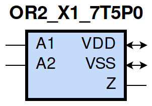
gf180mcu_fd_sc_mcu7t5v0__or2_1 symbol
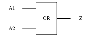
gf180mcu_fd_sc_mcu7t5v0__or2_1 schematic

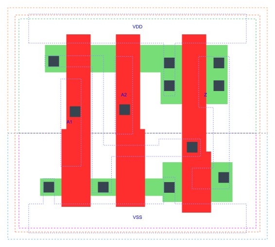
gf180mcu_fd_sc_mcu7t5v0__or2_1 layout
OR2_X1 is a 2-input OR(A1,A2), 1X drive strength
Attribute |
Value |
area |
17.561600 µm2 |
Output Pin |
Function |
Z |
(A1|A2) |
A1 |
A2 |
Z |
1 |
? |
1 |
? |
1 |
1 |
0 |
0 |
0 |
Pin |
Type |
Capacitance (pf) |
A1 |
input |
0.0029 |
A2 |
input |
0.0028 |
Input Pin |
Output |
When Condition |
Tin (ns) |
Out Load (pf) |
Delay (ns) |
Tout (ns) |
A1(LH) |
Z(LH) |
!A2 |
0.0100 |
0.0010 |
0.1693 |
0.0412 |
A1(HL) |
Z(HL) |
!A2 |
0.0100 |
0.0010 |
0.3122 |
0.0615 |
A2(HL) |
Z(HL) |
!A1 |
0.0100 |
0.0010 |
0.3392 |
0.0614 |
A2(LH) |
Z(LH) |
!A1 |
0.0100 |
0.0010 |
0.1869 |
0.0422 |
Input Pin |
When Condition |
Tin (ns) |
Output |
Out Load (pf) |
Energy (uW/MHz) |
A2 |
!A1 |
0.0100 |
Z(HL) |
0.0010 |
0.2462 |
A2 |
!A1 |
0.0100 |
Z(LH) |
0.0010 |
0.1241 |
A1 |
!A2 |
0.0100 |
Z(LH) |
0.0010 |
0.1103 |
A1 |
!A2 |
0.0100 |
Z(HL) |
0.0010 |
0.2323 |
A2(LH) |
A1 |
0.0100 |
n/a |
n/a |
-0.0151 |
A1(LH) |
A2 |
0.0100 |
n/a |
n/a |
-0.0051 |
A1(HL) |
A2 |
0.0100 |
n/a |
n/a |
0.0135 |
A2(HL) |
A1 |
0.0100 |
n/a |
n/a |
0.0181 |
When Condition |
Power (nW) |
!A1&!A2 |
0.1317 |
!A1&A2 |
0.1376 |
A1&!A2 |
0.1015 |
A1&A2 |
0.1015 |