gf180mcu_fd_sc_mcu9t5v0__xnor2_2
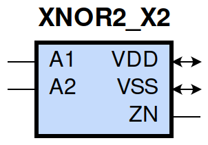
gf180mcu_fd_sc_mcu9t5v0__xnor2_2 symbol
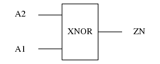
gf180mcu_fd_sc_mcu9t5v0__xnor2_2 schematic

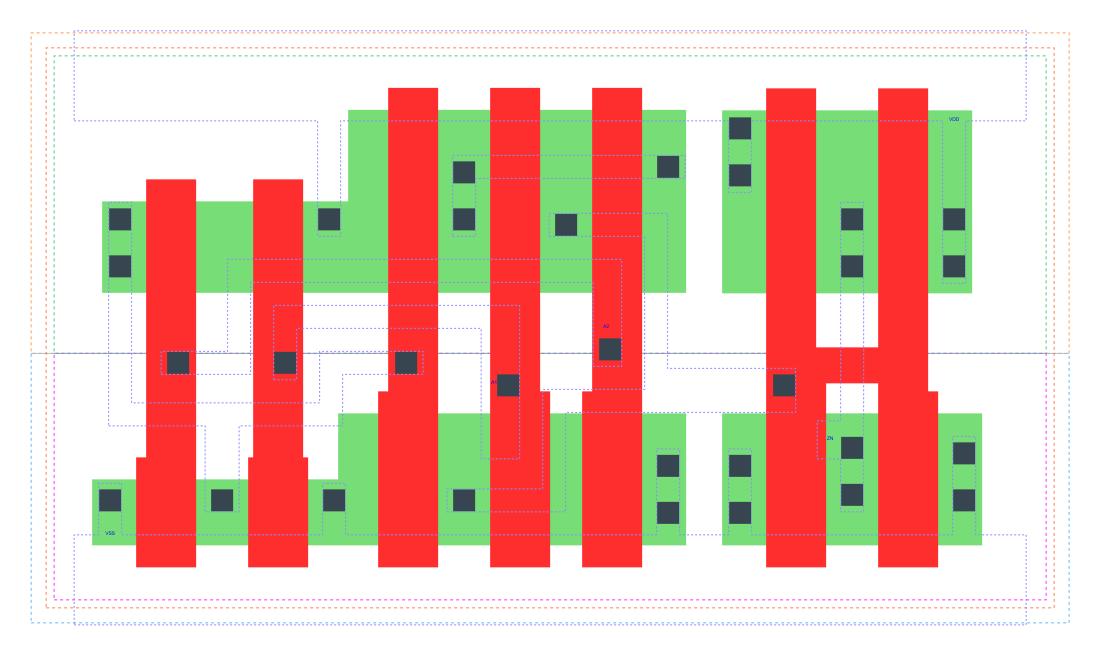
gf180mcu_fd_sc_mcu9t5v0__xnor2_2 layout
Attribute |
Value |
area |
47.980800 µm2 |
Output Pin |
Function |
ZN |
(!(A1^A2)) |
A1 |
A2 |
ZN |
1 |
1 |
1 |
0 |
0 |
1 |
1 |
0 |
0 |
0 |
1 |
0 |
Pin |
Type |
Capacitance (pf) |
A2 |
input |
0.0104 |
A1 |
input |
0.0109 |
Input Pin |
Output |
When Condition |
Tin (ns) |
Out Load (pf) |
Delay (ns) |
Tout (ns) |
A2(LH) |
ZN(LH) |
A1 |
0.0100 |
0.0010 |
0.1864 |
0.0302 |
A2(HL) |
ZN(LH) |
!A1 |
0.0100 |
0.0010 |
0.4467 |
0.0290 |
A2(HL) |
ZN(HL) |
A1 |
0.0100 |
0.0010 |
0.2629 |
0.0439 |
A2(LH) |
ZN(HL) |
!A1 |
0.0100 |
0.0010 |
0.3533 |
0.0397 |
A1(HL) |
ZN(LH) |
!A2 |
0.0100 |
0.0010 |
0.4732 |
0.0290 |
A1(HL) |
ZN(HL) |
A2 |
0.0100 |
0.0010 |
0.2343 |
0.0394 |
A1(LH) |
ZN(HL) |
!A2 |
0.0100 |
0.0010 |
0.4021 |
0.0442 |
A1(LH) |
ZN(LH) |
A2 |
0.0100 |
0.0010 |
0.1750 |
0.0304 |
Input Pin |
When Condition |
Tin (ns) |
Output |
Out Load (pf) |
Energy (uW/MHz) |
A2 |
A1 |
0.0100 |
ZN(LH) |
0.0010 |
0.2842 |
A2 |
!A1 |
0.0100 |
ZN(LH) |
0.0010 |
0.7026 |
A1 |
!A2 |
0.0100 |
ZN(LH) |
0.0010 |
0.7293 |
A1 |
A2 |
0.0100 |
ZN(LH) |
0.0010 |
0.2679 |
A1 |
A2 |
0.0100 |
ZN(HL) |
0.0010 |
0.6228 |
A1 |
!A2 |
0.0100 |
ZN(HL) |
0.0010 |
0.7419 |
A2 |
A1 |
0.0100 |
ZN(HL) |
0.0010 |
0.7029 |
A2 |
!A1 |
0.0100 |
ZN(HL) |
0.0010 |
0.6297 |
When Condition |
Power (nW) |
!A1&!A2 |
0.2575 |
A1&A2 |
0.1812 |
!A1&A2 |
0.1812 |
A1&!A2 |
0.2567 |