gf180mcu_fd_sc_mcu9t5v0__oai21_1
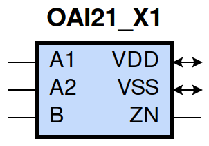
gf180mcu_fd_sc_mcu9t5v0__oai21_1 symbol
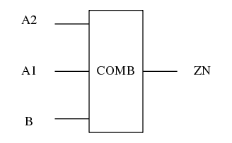
gf180mcu_fd_sc_mcu9t5v0__oai21_1 schematic

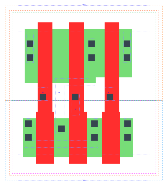
gf180mcu_fd_sc_mcu9t5v0__oai21_1 layout
Attribute |
Value |
area |
22.579200 µm2 |
Output Pin |
Function |
ZN |
(((!A1)&(!A2))|(!B)) |
A1 |
A2 |
B |
ZN |
0 |
0 |
? |
1 |
? |
? |
0 |
1 |
1 |
? |
1 |
0 |
? |
1 |
1 |
0 |
Pin |
Type |
Capacitance (pf) |
A2 |
input |
0.0066 |
A1 |
input |
0.0070 |
B |
input |
0.0064 |
Input Pin |
Output |
When Condition |
Tin (ns) |
Out Load (pf) |
Delay (ns) |
Tout (ns) |
A2(HL) |
ZN(LH) |
!A1&B |
0.0100 |
0.0010 |
0.1196 |
0.0704 |
A2(LH) |
ZN(HL) |
!A1&B |
0.0100 |
0.0010 |
0.0729 |
0.0465 |
A1(HL) |
ZN(LH) |
!A2&B |
0.0100 |
0.0010 |
0.0956 |
0.0700 |
A1(LH) |
ZN(HL) |
!A2&B |
0.0100 |
0.0010 |
0.0542 |
0.0310 |
B(LH) |
ZN(HL) |
!A1&A2 |
0.0100 |
0.0010 |
0.0957 |
0.0461 |
B(LH) |
ZN(HL) |
A1&!A2 |
0.0100 |
0.0010 |
0.0747 |
0.0315 |
B(LH) |
ZN(HL) |
A1&A2 |
0.0100 |
0.0010 |
0.0651 |
0.0308 |
B(HL) |
ZN(LH) |
!A1&A2 |
0.0100 |
0.0010 |
0.1030 |
0.0913 |
B(HL) |
ZN(LH) |
A1&!A2 |
0.0100 |
0.0010 |
0.0968 |
0.0681 |
B(HL) |
ZN(LH) |
A1&A2 |
0.0100 |
0.0010 |
0.1129 |
0.0793 |
Input Pin |
When Condition |
Tin (ns) |
Output |
Out Load (pf) |
Energy (uW/MHz) |
A1 |
!A2&B |
0.0100 |
ZN(LH) |
0.0010 |
0.1655 |
B |
!A1&A2 |
0.0100 |
ZN(HL) |
0.0010 |
0.0475 |
B |
A1&!A2 |
0.0100 |
ZN(HL) |
0.0010 |
0.0097 |
B |
A1&A2 |
0.0100 |
ZN(HL) |
0.0010 |
0.0098 |
A2 |
!A1&B |
0.0100 |
ZN(LH) |
0.0010 |
0.2102 |
A1 |
!A2&B |
0.0100 |
ZN(HL) |
0.0010 |
0.0098 |
B |
!A1&A2 |
0.0100 |
ZN(LH) |
0.0010 |
0.3149 |
B |
A1&!A2 |
0.0100 |
ZN(LH) |
0.0010 |
0.2704 |
B |
A1&A2 |
0.0100 |
ZN(LH) |
0.0010 |
0.3065 |
A2 |
!A1&B |
0.0100 |
ZN(HL) |
0.0010 |
0.0429 |
B(HL) |
!A1&!A2 |
0.0100 |
n/a |
n/a |
0.0621 |
A2(LH) |
!A1&!B |
0.0100 |
n/a |
n/a |
0.0041 |
A2(LH) |
A1&!B |
0.0100 |
n/a |
n/a |
-0.0649 |
A2(LH) |
A1&B |
0.0100 |
n/a |
n/a |
-0.0498 |
A1(LH) |
!A2&!B |
0.0100 |
n/a |
n/a |
0.0036 |
A1(LH) |
A2&!B |
0.0100 |
n/a |
n/a |
-0.0657 |
A1(LH) |
A2&B |
0.0100 |
n/a |
n/a |
-0.0169 |
A2(HL) |
!A1&!B |
0.0100 |
n/a |
n/a |
0.0670 |
A2(HL) |
A1&!B |
0.0100 |
n/a |
n/a |
0.0705 |
A2(HL) |
A1&B |
0.0100 |
n/a |
n/a |
0.0596 |
B(LH) |
!A1&!A2 |
0.0100 |
n/a |
n/a |
-0.0539 |
A1(HL) |
!A2&!B |
0.0100 |
n/a |
n/a |
0.0674 |
A1(HL) |
A2&!B |
0.0100 |
n/a |
n/a |
0.0707 |
A1(HL) |
A2&B |
0.0100 |
n/a |
n/a |
0.0397 |
When Condition |
Power (nW) |
!A1&!A2&!B |
0.1004 |
!A1&!A2&B |
0.1012 |
!A1&A2&!B |
0.1602 |
A1&!A2&!B |
0.1602 |
A1&A2&!B |
0.1605 |
!A1&A2&B |
0.1391 |
A1&!A2&B |
0.1036 |
A1&A2&B |
0.1036 |