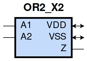
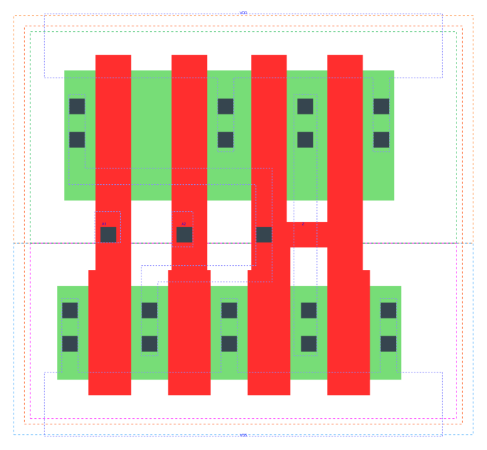
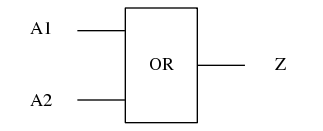
gf180mcu_fd_sc_mcu9t5v0__or2_2
gf180mcu_fd_sc_mcu9t5v0__or2_2 symbol
gf180mcu_fd_sc_mcu9t5v0__or2_2 schematic

gf180mcu_fd_sc_mcu9t5v0__or2_2 layout
Attribute |
Value |
area |
28.224000 µm2 |
Output Pin |
Function |
Z |
(A1|A2) |
A1 |
A2 |
Z |
1 |
? |
1 |
? |
1 |
1 |
0 |
0 |
0 |
Pin |
Type |
Capacitance (pf) |
A1 |
input |
0.0068 |
A2 |
input |
0.0067 |
Input Pin |
Output |
When Condition |
Tin (ns) |
Out Load (pf) |
Delay (ns) |
Tout (ns) |
A1(LH) |
Z(LH) |
!A2 |
0.0100 |
0.0010 |
0.1258 |
0.0245 |
A1(HL) |
Z(HL) |
!A2 |
0.0100 |
0.0010 |
0.2296 |
0.0391 |
A2(HL) |
Z(HL) |
!A1 |
0.0100 |
0.0010 |
0.2539 |
0.0391 |
A2(LH) |
Z(LH) |
!A1 |
0.0100 |
0.0010 |
0.1426 |
0.0255 |
Input Pin |
When Condition |
Tin (ns) |
Output |
Out Load (pf) |
Energy (uW/MHz) |
A2 |
!A1 |
0.0100 |
Z(HL) |
0.0010 |
0.6127 |
A2 |
!A1 |
0.0100 |
Z(LH) |
0.0010 |
0.2987 |
A1 |
!A2 |
0.0100 |
Z(LH) |
0.0010 |
0.2581 |
A1 |
!A2 |
0.0100 |
Z(HL) |
0.0010 |
0.5681 |
A2(LH) |
A1 |
0.0100 |
n/a |
n/a |
-0.0496 |
A1(LH) |
A2 |
0.0100 |
n/a |
n/a |
-0.0167 |
A1(HL) |
A2 |
0.0100 |
n/a |
n/a |
0.0395 |
A2(HL) |
A1 |
0.0100 |
n/a |
n/a |
0.0593 |
When Condition |
Power (nW) |
!A1&!A2 |
0.1549 |
!A1&A2 |
0.1635 |
A1&!A2 |
0.1280 |
A1&A2 |
0.1280 |