gf180mcu_fd_sc_mcu9t5v0__and2_2
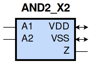
gf180mcu_fd_sc_mcu9t5v0__and2_2 symbol
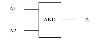
gf180mcu_fd_sc_mcu9t5v0__and2_2 schematic

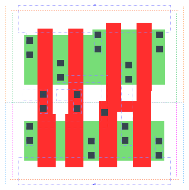
gf180mcu_fd_sc_mcu9t5v0__and2_2 layout
Attribute |
Value |
area |
25.401600 µm2 |
Output Pin |
Function |
Z |
(A1&A2) |
A1 |
A2 |
Z |
1 |
1 |
1 |
0 |
? |
0 |
? |
0 |
0 |
Pin |
Type |
Capacitance (pf) |
A1 |
input |
0.0067 |
A2 |
input |
0.0066 |
Input Pin |
Output |
When Condition |
Tin (ns) |
Out Load (pf) |
Delay (ns) |
Tout (ns) |
A1(LH) |
Z(LH) |
A2 |
0.0100 |
0.0010 |
0.1659 |
0.0293 |
A1(HL) |
Z(HL) |
A2 |
0.0100 |
0.0010 |
0.1572 |
0.0266 |
A2(HL) |
Z(HL) |
A1 |
0.0100 |
0.0010 |
0.1752 |
0.0297 |
A2(LH) |
Z(LH) |
A1 |
0.0100 |
0.0010 |
0.1773 |
0.0295 |
Input Pin |
When Condition |
Tin (ns) |
Output |
Out Load (pf) |
Energy (uW/MHz) |
A2 |
A1 |
0.0100 |
Z(HL) |
0.0010 |
0.5511 |
A2 |
A1 |
0.0100 |
Z(LH) |
0.0010 |
0.2863 |
A1 |
A2 |
0.0100 |
Z(LH) |
0.0010 |
0.2860 |
A1 |
A2 |
0.0100 |
Z(HL) |
0.0010 |
0.4777 |
A2(LH) |
!A1 |
0.0100 |
n/a |
n/a |
-0.0532 |
A1(LH) |
!A2 |
0.0100 |
n/a |
n/a |
-0.0382 |
A1(HL) |
!A2 |
0.0100 |
n/a |
n/a |
0.0607 |
A2(HL) |
!A1 |
0.0100 |
n/a |
n/a |
0.0601 |
When Condition |
Power (nW) |
!A1&!A2 |
0.1290 |
!A1&A2 |
0.1293 |
A1&!A2 |
0.1691 |
A1&A2 |
0.1547 |