gf180mcu_fd_sc_mcu9t5v0__nand2_2
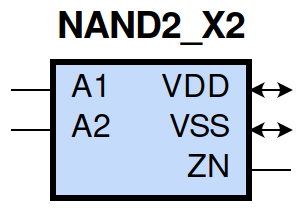
gf180mcu_fd_sc_mcu9t5v0__nand2_2 symbol
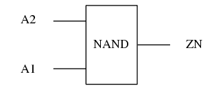
gf180mcu_fd_sc_mcu9t5v0__nand2_2 schematic

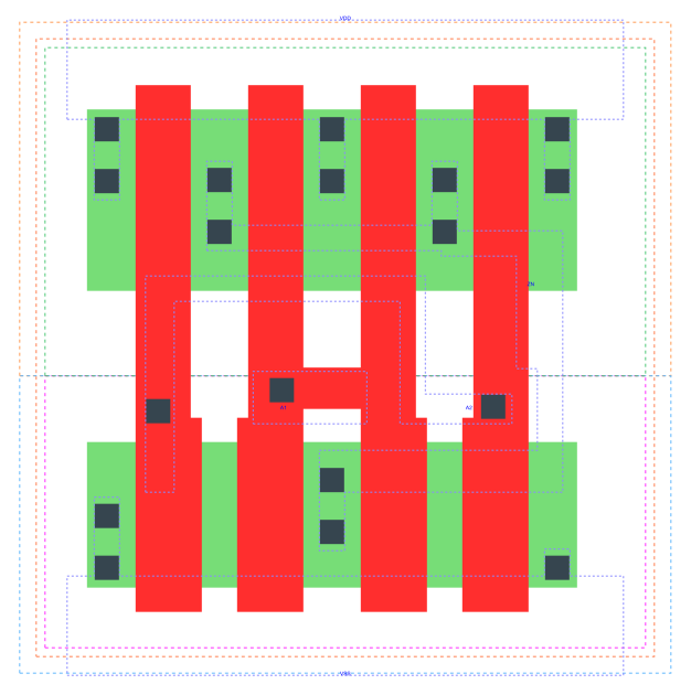
gf180mcu_fd_sc_mcu9t5v0__nand2_2 layout
Attribute |
Value |
area |
25.401600 µm2 |
Output Pin |
Function |
ZN |
((!A1)|(!A2)) |
A1 |
A2 |
ZN |
0 |
? |
1 |
? |
0 |
1 |
1 |
1 |
0 |
Pin |
Type |
Capacitance (pf) |
A2 |
input |
0.0137 |
A1 |
input |
0.0130 |
Input Pin |
Output |
When Condition |
Tin (ns) |
Out Load (pf) |
Delay (ns) |
Tout (ns) |
A2(HL) |
ZN(LH) |
A1 |
0.0100 |
0.0010 |
0.0688 |
0.0461 |
A2(LH) |
ZN(HL) |
A1 |
0.0100 |
0.0010 |
0.0552 |
0.0229 |
A1(HL) |
ZN(LH) |
A2 |
0.0100 |
0.0010 |
0.0484 |
0.0286 |
A1(LH) |
ZN(HL) |
A2 |
0.0100 |
0.0010 |
0.0439 |
0.0228 |
Input Pin |
When Condition |
Tin (ns) |
Output |
Out Load (pf) |
Energy (uW/MHz) |
A1 |
A2 |
0.0100 |
ZN(LH) |
0.0010 |
0.2735 |
A2 |
A1 |
0.0100 |
ZN(LH) |
0.0010 |
0.3939 |
A1 |
A2 |
0.0100 |
ZN(HL) |
0.0010 |
0.0010 |
A2 |
A1 |
0.0100 |
ZN(HL) |
0.0010 |
0.0010 |
A2(LH) |
!A1 |
0.0100 |
n/a |
n/a |
-0.1075 |
A1(LH) |
!A2 |
0.0100 |
n/a |
n/a |
-0.0773 |
A2(HL) |
!A1 |
0.0100 |
n/a |
n/a |
0.1211 |
A1(HL) |
!A2 |
0.0100 |
n/a |
n/a |
0.1229 |
When Condition |
Power (nW) |
!A1&!A2 |
0.1005 |
!A1&A2 |
0.1012 |
A1&!A2 |
0.1807 |
A1&A2 |
0.1570 |