gf180mcu_fd_sc_mcu9t5v0__xor2_4
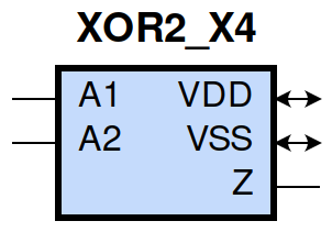
gf180mcu_fd_sc_mcu9t5v0__xor2_4 symbol
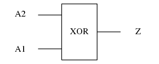
gf180mcu_fd_sc_mcu9t5v0__xor2_4 schematic

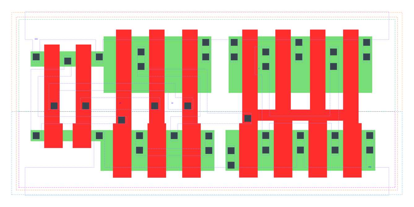
gf180mcu_fd_sc_mcu9t5v0__xor2_4 layout
Attribute |
Value |
area |
59.270400 µm2 |
Output Pin |
Function |
Z |
(A1^A2) |
A1 |
A2 |
Z |
1 |
0 |
1 |
0 |
1 |
1 |
1 |
1 |
0 |
0 |
0 |
0 |
Pin |
Type |
Capacitance (pf) |
A2 |
input |
0.0095 |
A1 |
input |
0.0095 |
Input Pin |
Output |
When Condition |
Tin (ns) |
Out Load (pf) |
Delay (ns) |
Tout (ns) |
A2(HL) |
Z(HL) |
!A1 |
0.0100 |
0.0010 |
0.3757 |
0.0574 |
A2(LH) |
Z(LH) |
!A1 |
0.0100 |
0.0010 |
0.2781 |
0.0407 |
A2(HL) |
Z(LH) |
A1 |
0.0100 |
0.0010 |
0.5020 |
0.0405 |
A2(LH) |
Z(HL) |
A1 |
0.0100 |
0.0010 |
0.4798 |
0.0437 |
A1(LH) |
Z(HL) |
A2 |
0.0100 |
0.0010 |
0.4920 |
0.0436 |
A1(HL) |
Z(LH) |
A2 |
0.0100 |
0.0010 |
0.5478 |
0.0416 |
A1(LH) |
Z(LH) |
!A2 |
0.0100 |
0.0010 |
0.2496 |
0.0392 |
A1(HL) |
Z(HL) |
!A2 |
0.0100 |
0.0010 |
0.3518 |
0.0574 |
Input Pin |
When Condition |
Tin (ns) |
Output |
Out Load (pf) |
Energy (uW/MHz) |
A2 |
!A1 |
0.0100 |
Z(HL) |
0.0010 |
1.3649 |
A2 |
A1 |
0.0100 |
Z(HL) |
0.0010 |
1.1806 |
A1 |
A2 |
0.0100 |
Z(HL) |
0.0010 |
1.2189 |
A1 |
!A2 |
0.0100 |
Z(HL) |
0.0010 |
1.3205 |
A2 |
!A1 |
0.0100 |
Z(LH) |
0.0010 |
0.8068 |
A2 |
A1 |
0.0100 |
Z(LH) |
0.0010 |
1.0702 |
A1 |
A2 |
0.0100 |
Z(LH) |
0.0010 |
1.1478 |
A1 |
!A2 |
0.0100 |
Z(LH) |
0.0010 |
0.7343 |
When Condition |
Power (nW) |
!A1&!A2 |
0.2342 |
A1&A2 |
0.3199 |
!A1&A2 |
0.3093 |
A1&!A2 |
0.2336 |