gf180mcu_fd_sc_mcu9t5v0__bufz_x12
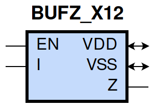
gf180mcu_fd_sc_mcu9t5v0__bufz_x12 symbol
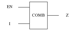
gf180mcu_fd_sc_mcu9t5v0__bufz_x12 schematic

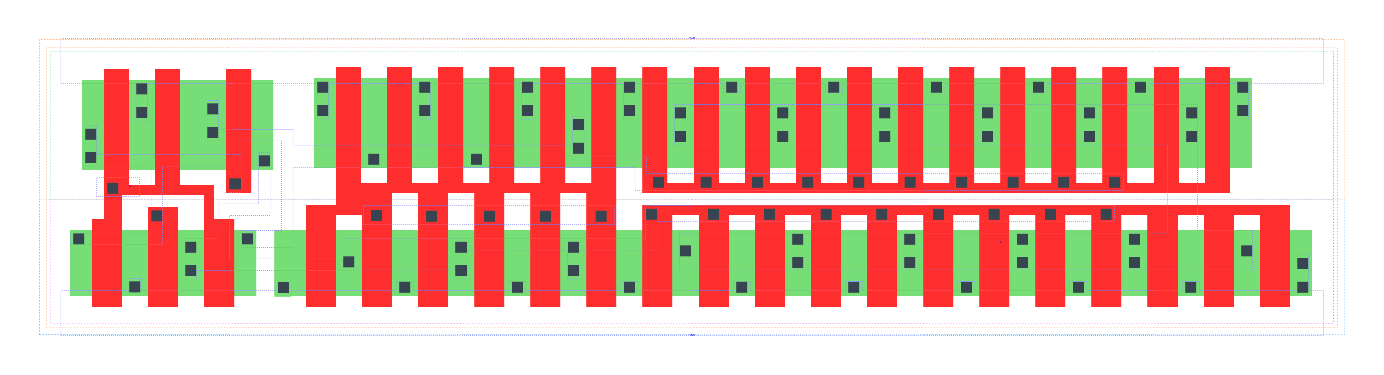
gf180mcu_fd_sc_mcu9t5v0__bufz_x12 layout
Attribute |
Value |
area |
127.008000 µm2 |
Output Pin |
Function |
Z |
I |
EN |
I |
Z |
1 |
1 |
1 |
1 |
0 |
0 |
0 |
? |
z |
Pin |
Type |
Capacitance (pf) |
EN |
input |
0.0136 |
I |
input |
0.0402 |
Input Pin |
Output |
When Condition |
Tin (ns) |
Out Load (pf) |
Delay (ns) |
Tout (ns) |
EN(LH) |
Z(ZL) |
!I |
0.0100 |
0.0010 |
0.1655 |
0.0402 |
EN(LH) |
Z(ZH) |
I |
0.0100 |
0.0010 |
0.1891 |
0.0467 |
EN(HL) |
Z(LZ) |
!I |
0.0100 |
0.3470 |
0.0000 |
|
EN(HL) |
Z(HZ) |
I |
0.0100 |
0.4040 |
0.0000 |
|
I(HL) |
Z(HL) |
EN |
0.0100 |
0.0010 |
0.2117 |
0.0383 |
I(LH) |
Z(LH) |
EN |
0.0100 |
0.0010 |
0.2363 |
0.0438 |
Input Pin |
When Condition |
Tin (ns) |
Output |
Out Load (pf) |
Energy (uW/MHz) |
I |
EN |
0.0100 |
Z(HL) |
0.0010 |
2.4587 |
I |
EN |
0.0100 |
Z(LH) |
0.0010 |
1.3190 |
EN(HL) |
!I |
0.0100 |
n/a |
n/a |
0.3662 |
EN(HL) |
I |
0.0100 |
n/a |
n/a |
0.7006 |
I(LH) |
!EN |
0.0100 |
n/a |
n/a |
-0.3499 |
EN |
I |
0.0100 |
Z(LH) |
0.0010 |
1.4014 |
I(HL) |
!EN |
0.0100 |
n/a |
n/a |
0.3524 |
EN |
!I |
0.0100 |
Z(HL) |
0.0010 |
1.5291 |
When Condition |
Power (nW) |
!EN&!I |
0.2848 |
!EN&I |
0.2848 |
EN&!I |
0.6280 |
EN&I |
0.6217 |