gf180mcu_fd_sc_mcu9t5v0__bufz_x16
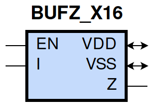
gf180mcu_fd_sc_mcu9t5v0__bufz_x16 symbol
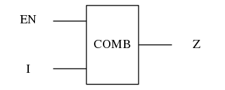
gf180mcu_fd_sc_mcu9t5v0__bufz_x16 schematic

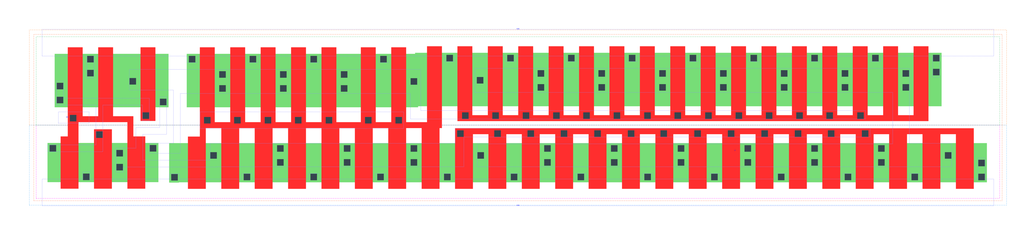
gf180mcu_fd_sc_mcu9t5v0__bufz_x16 layout
Attribute |
Value |
area |
160.876800 µm2 |
Output Pin |
Function |
Z |
I |
EN |
I |
Z |
1 |
1 |
1 |
1 |
0 |
0 |
0 |
? |
z |
Pin |
Type |
Capacitance (pf) |
EN |
input |
0.0137 |
I |
input |
0.0530 |
Input Pin |
Output |
When Condition |
Tin (ns) |
Out Load (pf) |
Delay (ns) |
Tout (ns) |
EN(LH) |
Z(ZL) |
!I |
0.0100 |
0.0010 |
0.1849 |
0.0457 |
EN(LH) |
Z(ZH) |
I |
0.0100 |
0.0010 |
0.2211 |
0.0542 |
EN(HL) |
Z(LZ) |
!I |
0.0100 |
0.4170 |
0.0000 |
|
EN(HL) |
Z(HZ) |
I |
0.0100 |
0.5300 |
0.0000 |
|
I(HL) |
Z(HL) |
EN |
0.0100 |
0.0010 |
0.2362 |
0.0430 |
I(LH) |
Z(LH) |
EN |
0.0100 |
0.0010 |
0.2754 |
0.0509 |
Input Pin |
When Condition |
Tin (ns) |
Output |
Out Load (pf) |
Energy (uW/MHz) |
I |
EN |
0.0100 |
Z(HL) |
0.0010 |
3.2105 |
I |
EN |
0.0100 |
Z(LH) |
0.0010 |
1.7621 |
EN(HL) |
!I |
0.0100 |
n/a |
n/a |
0.3683 |
EN(HL) |
I |
0.0100 |
n/a |
n/a |
0.8109 |
I(LH) |
!EN |
0.0100 |
n/a |
n/a |
-0.4670 |
EN |
I |
0.0100 |
Z(LH) |
0.0010 |
1.8856 |
I(HL) |
!EN |
0.0100 |
n/a |
n/a |
0.4690 |
EN |
!I |
0.0100 |
Z(HL) |
0.0010 |
1.9994 |
When Condition |
Power (nW) |
!EN&!I |
0.3373 |
!EN&I |
0.3373 |
EN&!I |
0.7865 |
EN&I |
0.7777 |