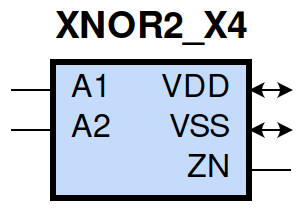
gf180mcu_fd_sc_mcu9t5v0__xnor2_4
gf180mcu_fd_sc_mcu9t5v0__xnor2_4 symbol
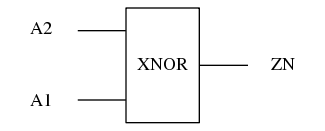
gf180mcu_fd_sc_mcu9t5v0__xnor2_4 schematic

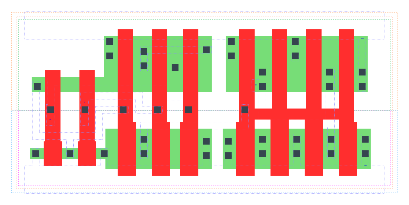
gf180mcu_fd_sc_mcu9t5v0__xnor2_4 layout
Attribute |
Value |
area |
59.270400 µm2 |
Output Pin |
Function |
ZN |
(!(A1^A2)) |
A1 |
A2 |
ZN |
1 |
1 |
1 |
0 |
0 |
1 |
1 |
0 |
0 |
0 |
1 |
0 |
Pin |
Type |
Capacitance (pf) |
A2 |
input |
0.0094 |
A1 |
input |
0.0096 |
Input Pin |
Output |
When Condition |
Tin (ns) |
Out Load (pf) |
Delay (ns) |
Tout (ns) |
A2(LH) |
ZN(LH) |
A1 |
0.0100 |
0.0010 |
0.2620 |
0.0383 |
A2(HL) |
ZN(LH) |
!A1 |
0.0100 |
0.0010 |
0.6781 |
0.0377 |
A2(HL) |
ZN(HL) |
A1 |
0.0100 |
0.0010 |
0.3721 |
0.0612 |
A2(LH) |
ZN(HL) |
!A1 |
0.0100 |
0.0010 |
0.5056 |
0.0573 |
A1(HL) |
ZN(LH) |
!A2 |
0.0100 |
0.0010 |
0.7074 |
0.0378 |
A1(HL) |
ZN(HL) |
A2 |
0.0100 |
0.0010 |
0.3454 |
0.0572 |
A1(LH) |
ZN(HL) |
!A2 |
0.0100 |
0.0010 |
0.5534 |
0.0611 |
A1(LH) |
ZN(LH) |
A2 |
0.0100 |
0.0010 |
0.2507 |
0.0385 |
Input Pin |
When Condition |
Tin (ns) |
Output |
Out Load (pf) |
Energy (uW/MHz) |
A2 |
A1 |
0.0100 |
ZN(LH) |
0.0010 |
0.7285 |
A2 |
!A1 |
0.0100 |
ZN(LH) |
0.0010 |
1.1941 |
A1 |
!A2 |
0.0100 |
ZN(LH) |
0.0010 |
1.2091 |
A1 |
A2 |
0.0100 |
ZN(LH) |
0.0010 |
0.7198 |
A1 |
A2 |
0.0100 |
ZN(HL) |
0.0010 |
1.3303 |
A1 |
!A2 |
0.0100 |
ZN(HL) |
0.0010 |
1.4941 |
A2 |
A1 |
0.0100 |
ZN(HL) |
0.0010 |
1.4496 |
A2 |
!A1 |
0.0100 |
ZN(HL) |
0.0010 |
1.3539 |
When Condition |
Power (nW) |
!A1&!A2 |
0.3129 |
A1&A2 |
0.2321 |
!A1&A2 |
0.2346 |
A1&!A2 |
0.3105 |