gf180mcu_fd_sc_mcu9t5v0__and2_1
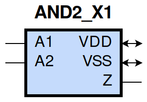
gf180mcu_fd_sc_mcu9t5v0__and2_1 symbol
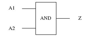
gf180mcu_fd_sc_mcu9t5v0__and2_1 schematic

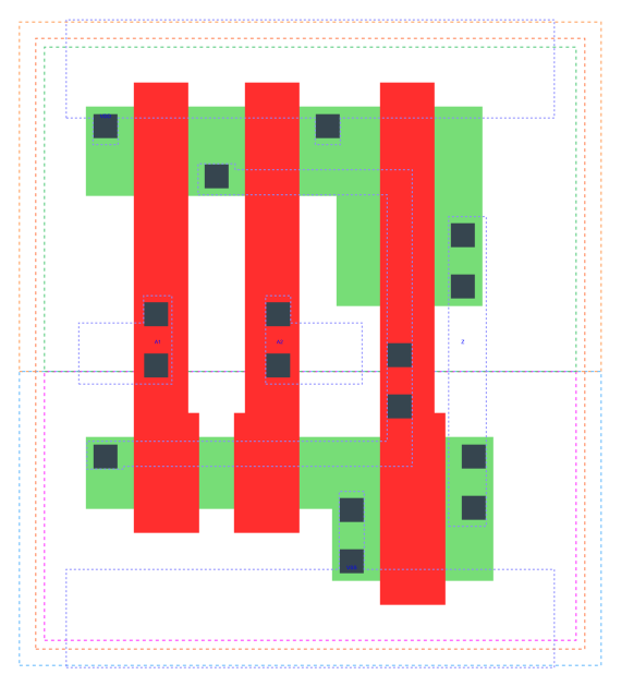
gf180mcu_fd_sc_mcu9t5v0__and2_1 layout
Attribute |
Value |
area |
22.579200 µm2 |
Output Pin |
Function |
Z |
(A1&A2) |
A1 |
A2 |
Z |
1 |
1 |
1 |
0 |
? |
0 |
? |
0 |
0 |
Pin |
Type |
Capacitance (pf) |
A1 |
input |
0.0039 |
A2 |
input |
0.0038 |
Input Pin |
Output |
When Condition |
Tin (ns) |
Out Load (pf) |
Delay (ns) |
Tout (ns) |
A1(LH) |
Z(LH) |
A2 |
0.0100 |
0.0010 |
0.1882 |
0.0394 |
A1(HL) |
Z(HL) |
A2 |
0.0100 |
0.0010 |
0.1824 |
0.0351 |
A2(HL) |
Z(HL) |
A1 |
0.0100 |
0.0010 |
0.2016 |
0.0385 |
A2(LH) |
Z(LH) |
A1 |
0.0100 |
0.0010 |
0.1993 |
0.0394 |
Input Pin |
When Condition |
Tin (ns) |
Output |
Out Load (pf) |
Energy (uW/MHz) |
A2 |
A1 |
0.0100 |
Z(HL) |
0.0010 |
0.3067 |
A2 |
A1 |
0.0100 |
Z(LH) |
0.0010 |
0.1614 |
A1 |
A2 |
0.0100 |
Z(LH) |
0.0010 |
0.1614 |
A1 |
A2 |
0.0100 |
Z(HL) |
0.0010 |
0.2695 |
A2(LH) |
!A1 |
0.0100 |
n/a |
n/a |
-0.0262 |
A1(LH) |
!A2 |
0.0100 |
n/a |
n/a |
-0.0178 |
A1(HL) |
!A2 |
0.0100 |
n/a |
n/a |
0.0300 |
A2(HL) |
!A1 |
0.0100 |
n/a |
n/a |
0.0297 |
When Condition |
Power (nW) |
!A1&!A2 |
0.1021 |
!A1&A2 |
0.1023 |
A1&!A2 |
0.1423 |
A1&A2 |
0.1281 |