gf180mcu_fd_sc_mcu9t5v0__or2_1
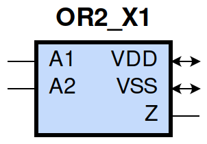
gf180mcu_fd_sc_mcu9t5v0__or2_1 symbol
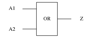
gf180mcu_fd_sc_mcu9t5v0__or2_1 schematic

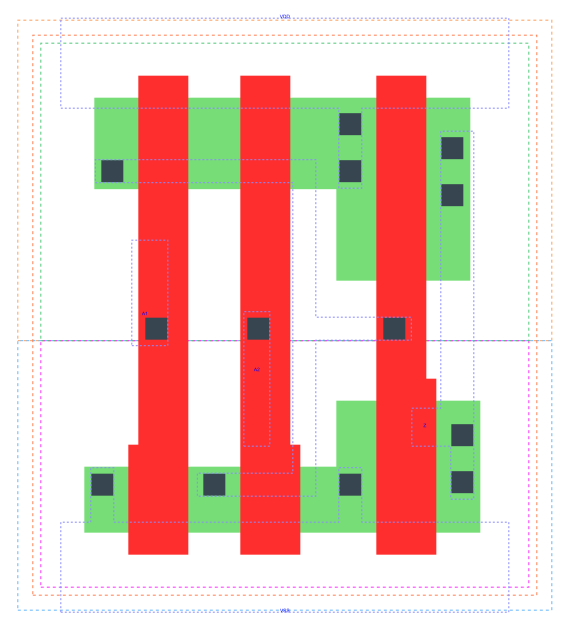
gf180mcu_fd_sc_mcu9t5v0__or2_1 layout
Attribute |
Value |
area |
22.579200 µm2 |
Output Pin |
Function |
Z |
(A1|A2) |
A1 |
A2 |
Z |
1 |
? |
1 |
? |
1 |
1 |
0 |
0 |
0 |
Pin |
Type |
Capacitance (pf) |
A1 |
input |
0.0040 |
A2 |
input |
0.0041 |
Input Pin |
Output |
When Condition |
Tin (ns) |
Out Load (pf) |
Delay (ns) |
Tout (ns) |
A1(LH) |
Z(LH) |
!A2 |
0.0100 |
0.0010 |
0.1434 |
0.0340 |
A1(HL) |
Z(HL) |
!A2 |
0.0100 |
0.0010 |
0.2666 |
0.0505 |
A2(HL) |
Z(HL) |
!A1 |
0.0100 |
0.0010 |
0.2917 |
0.0506 |
A2(LH) |
Z(LH) |
!A1 |
0.0100 |
0.0010 |
0.1594 |
0.0349 |
Input Pin |
When Condition |
Tin (ns) |
Output |
Out Load (pf) |
Energy (uW/MHz) |
A2 |
!A1 |
0.0100 |
Z(HL) |
0.0010 |
0.3400 |
A2 |
!A1 |
0.0100 |
Z(LH) |
0.0010 |
0.1711 |
A1 |
!A2 |
0.0100 |
Z(LH) |
0.0010 |
0.1512 |
A1 |
!A2 |
0.0100 |
Z(HL) |
0.0010 |
0.3179 |
A2(LH) |
A1 |
0.0100 |
n/a |
n/a |
-0.0245 |
A1(LH) |
A2 |
0.0100 |
n/a |
n/a |
-0.0083 |
A1(HL) |
A2 |
0.0100 |
n/a |
n/a |
0.0203 |
A2(HL) |
A1 |
0.0100 |
n/a |
n/a |
0.0292 |
When Condition |
Power (nW) |
!A1&!A2 |
0.1277 |
!A1&A2 |
0.1377 |
A1&!A2 |
0.1019 |
A1&A2 |
0.1019 |