gf180mcu_fd_sc_mcu9t5v0__xor3_2
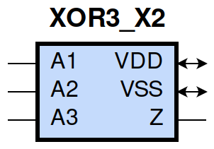
gf180mcu_fd_sc_mcu9t5v0__xor3_2 symbol
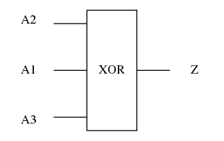
gf180mcu_fd_sc_mcu9t5v0__xor3_2 schematic

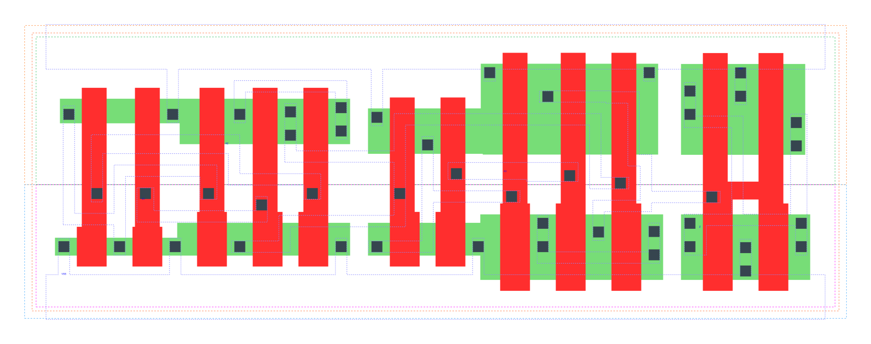
gf180mcu_fd_sc_mcu9t5v0__xor3_2 layout
Attribute |
Value |
area |
79.027200 µm2 |
Output Pin |
Function |
Z |
(A1^A2^A3) |
A1 |
A2 |
A3 |
Z |
1 |
1 |
1 |
1 |
1 |
0 |
0 |
1 |
0 |
1 |
0 |
1 |
0 |
0 |
1 |
1 |
1 |
1 |
0 |
0 |
1 |
0 |
1 |
0 |
0 |
1 |
1 |
0 |
0 |
0 |
0 |
0 |
Pin |
Type |
Capacitance (pf) |
A2 |
input |
0.0068 |
A1 |
input |
0.0065 |
A3 |
input |
0.0103 |
Input Pin |
Output |
When Condition |
Tin (ns) |
Out Load (pf) |
Delay (ns) |
Tout (ns) |
A2(HL) |
Z(HL) |
!A1&!A3 |
0.0100 |
0.0010 |
0.7714 |
0.0466 |
A2(HL) |
Z(HL) |
A1&A3 |
0.0100 |
0.0010 |
0.7846 |
0.0382 |
A2(LH) |
Z(LH) |
!A1&!A3 |
0.0100 |
0.0010 |
0.7424 |
0.0427 |
A2(LH) |
Z(LH) |
A1&A3 |
0.0100 |
0.0010 |
0.5658 |
0.0385 |
A2(HL) |
Z(LH) |
!A1&A3 |
0.0100 |
0.0010 |
0.8657 |
0.0383 |
A2(HL) |
Z(LH) |
A1&!A3 |
0.0100 |
0.0010 |
0.6381 |
0.0431 |
A2(LH) |
Z(HL) |
!A1&A3 |
0.0100 |
0.0010 |
0.8892 |
0.0383 |
A2(LH) |
Z(HL) |
A1&!A3 |
0.0100 |
0.0010 |
0.4726 |
0.0473 |
A1(LH) |
Z(HL) |
!A2&A3 |
0.0100 |
0.0010 |
0.9442 |
0.0383 |
A1(LH) |
Z(HL) |
A2&!A3 |
0.0100 |
0.0010 |
0.4612 |
0.0473 |
A1(HL) |
Z(LH) |
!A2&A3 |
0.0100 |
0.0010 |
0.8946 |
0.0384 |
A1(HL) |
Z(LH) |
A2&!A3 |
0.0100 |
0.0010 |
0.6009 |
0.0427 |
A1(LH) |
Z(LH) |
!A2&!A3 |
0.0100 |
0.0010 |
0.7976 |
0.0432 |
A1(LH) |
Z(LH) |
A2&A3 |
0.0100 |
0.0010 |
0.5544 |
0.0384 |
A1(HL) |
Z(HL) |
!A2&!A3 |
0.0100 |
0.0010 |
0.8003 |
0.0466 |
A1(HL) |
Z(HL) |
A2&A3 |
0.0100 |
0.0010 |
0.7478 |
0.0384 |
A3(LH) |
Z(LH) |
!A1&!A2 |
0.0100 |
0.0010 |
0.1870 |
0.0376 |
A3(LH) |
Z(LH) |
A1&A2 |
0.0100 |
0.0010 |
0.1870 |
0.0376 |
A3(HL) |
Z(LH) |
!A1&A2 |
0.0100 |
0.0010 |
0.3936 |
0.0400 |
A3(HL) |
Z(LH) |
A1&!A2 |
0.0100 |
0.0010 |
0.3936 |
0.0400 |
A3(HL) |
Z(HL) |
!A1&!A2 |
0.0100 |
0.0010 |
0.2552 |
0.0461 |
A3(HL) |
Z(HL) |
A1&A2 |
0.0100 |
0.0010 |
0.2549 |
0.0461 |
A3(LH) |
Z(HL) |
!A1&A2 |
0.0100 |
0.0010 |
0.3681 |
0.0385 |
A3(LH) |
Z(HL) |
A1&!A2 |
0.0100 |
0.0010 |
0.3681 |
0.0385 |
Input Pin |
When Condition |
Tin (ns) |
Output |
Out Load (pf) |
Energy (uW/MHz) |
A3 |
!A1&!A2 |
0.0100 |
Z(LH) |
0.0010 |
0.3152 |
A3 |
A1&A2 |
0.0100 |
Z(LH) |
0.0010 |
0.3151 |
A3 |
!A1&A2 |
0.0100 |
Z(LH) |
0.0010 |
0.7417 |
A3 |
A1&!A2 |
0.0100 |
Z(LH) |
0.0010 |
0.7418 |
A2 |
!A1&!A3 |
0.0100 |
Z(HL) |
0.0010 |
0.9305 |
A2 |
A1&A3 |
0.0100 |
Z(HL) |
0.0010 |
1.0508 |
A2 |
!A1&A3 |
0.0100 |
Z(HL) |
0.0010 |
1.0306 |
A2 |
A1&!A3 |
0.0100 |
Z(HL) |
0.0010 |
0.6914 |
A1 |
!A2&A3 |
0.0100 |
Z(HL) |
0.0010 |
1.0803 |
A1 |
A2&!A3 |
0.0100 |
Z(HL) |
0.0010 |
0.6829 |
A1 |
!A2&!A3 |
0.0100 |
Z(HL) |
0.0010 |
0.9450 |
A1 |
A2&A3 |
0.0100 |
Z(HL) |
0.0010 |
1.0179 |
A2 |
!A1&!A3 |
0.0100 |
Z(LH) |
0.0010 |
0.8384 |
A2 |
A1&A3 |
0.0100 |
Z(LH) |
0.0010 |
0.6623 |
A2 |
!A1&A3 |
0.0100 |
Z(LH) |
0.0010 |
0.9048 |
A2 |
A1&!A3 |
0.0100 |
Z(LH) |
0.0010 |
0.8679 |
A1 |
!A2&A3 |
0.0100 |
Z(LH) |
0.0010 |
0.9186 |
A1 |
A2&!A3 |
0.0100 |
Z(LH) |
0.0010 |
0.8255 |
A1 |
!A2&!A3 |
0.0100 |
Z(LH) |
0.0010 |
0.8973 |
A1 |
A2&A3 |
0.0100 |
Z(LH) |
0.0010 |
0.6534 |
A3 |
!A1&!A2 |
0.0100 |
Z(HL) |
0.0010 |
0.6361 |
A3 |
A1&A2 |
0.0100 |
Z(HL) |
0.0010 |
0.6360 |
A3 |
!A1&A2 |
0.0100 |
Z(HL) |
0.0010 |
0.6749 |
A3 |
A1&!A2 |
0.0100 |
Z(HL) |
0.0010 |
0.6749 |
When Condition |
Power (nW) |
!A1&!A2&!A3 |
0.3405 |
!A1&A2&A3 |
0.3438 |
A1&!A2&A3 |
0.4199 |
A1&A2&!A3 |
0.2588 |
!A1&!A2&A3 |
0.3408 |
!A1&A2&!A3 |
0.3327 |
A1&!A2&!A3 |
0.4088 |
A1&A2&A3 |
0.2590 |