gf180mcu_fd_sc_mcu9t5v0__invz_x16
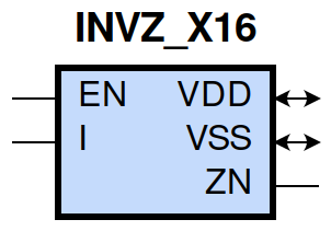
gf180mcu_fd_sc_mcu9t5v0__invz_x16 symbol
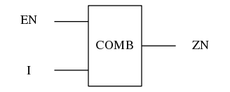
gf180mcu_fd_sc_mcu9t5v0__invz_x16 schematic

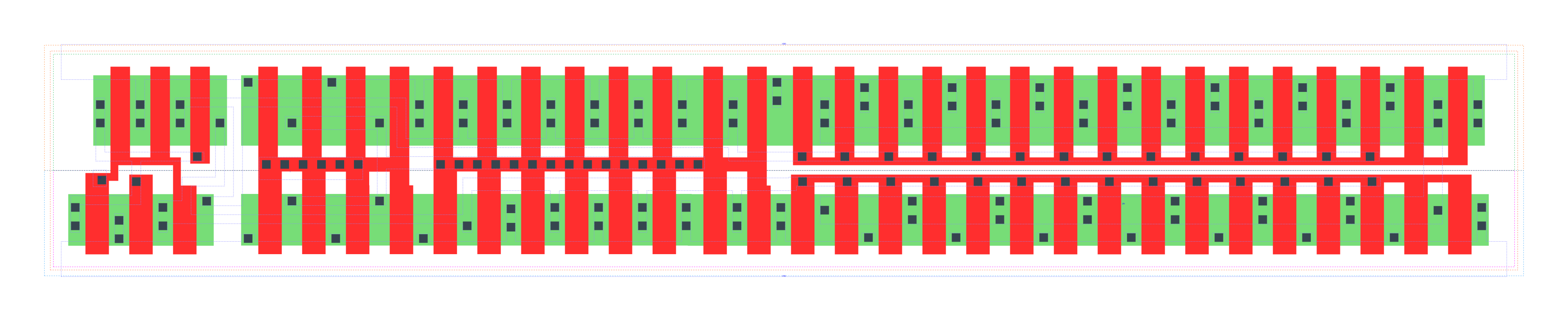
gf180mcu_fd_sc_mcu9t5v0__invz_x16 layout
Attribute |
Value |
area |
186.278400 µm2 |
Output Pin |
Function |
ZN |
(!I) |
EN |
I |
ZN |
1 |
0 |
1 |
1 |
1 |
0 |
0 |
? |
z |
Pin |
Type |
Capacitance (pf) |
EN |
input |
0.0137 |
I |
input |
0.0266 |
Input Pin |
Output |
When Condition |
Tin (ns) |
Out Load (pf) |
Delay (ns) |
Tout (ns) |
EN(LH) |
ZN(ZL) |
I |
0.0100 |
0.0010 |
0.1877 |
0.0463 |
EN(LH) |
ZN(ZH) |
!I |
0.0100 |
0.0010 |
0.2272 |
0.0559 |
EN(HL) |
ZN(HZ) |
!I |
0.0100 |
0.5500 |
0.0000 |
|
EN(HL) |
ZN(LZ) |
I |
0.0100 |
0.4220 |
0.0000 |
|
I(LH) |
ZN(HL) |
EN |
0.0100 |
0.0010 |
0.3110 |
0.0440 |
I(HL) |
ZN(LH) |
EN |
0.0100 |
0.0010 |
0.3849 |
0.0528 |
Input Pin |
When Condition |
Tin (ns) |
Output |
Out Load (pf) |
Energy (uW/MHz) |
I |
EN |
0.0100 |
ZN(HL) |
0.0010 |
3.2382 |
I |
EN |
0.0100 |
ZN(LH) |
0.0010 |
3.3619 |
EN |
I |
0.0100 |
ZN(HL) |
0.0010 |
2.0436 |
EN(HL) |
I |
0.0100 |
n/a |
n/a |
0.3721 |
EN(HL) |
!I |
0.0100 |
n/a |
n/a |
0.8279 |
EN |
!I |
0.0100 |
ZN(LH) |
0.0010 |
1.9220 |
I(LH) |
!EN |
0.0100 |
n/a |
n/a |
0.4142 |
I(HL) |
!EN |
0.0100 |
n/a |
n/a |
1.0985 |
When Condition |
Power (nW) |
!EN&!I |
0.4397 |
!EN&I |
0.4447 |
EN&!I |
0.8800 |
EN&I |
0.8938 |