gf180mcu_fd_sc_mcu9t5v0__oai21_4
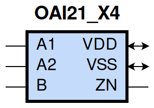
gf180mcu_fd_sc_mcu9t5v0__oai21_4 symbol
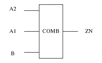
gf180mcu_fd_sc_mcu9t5v0__oai21_4 schematic

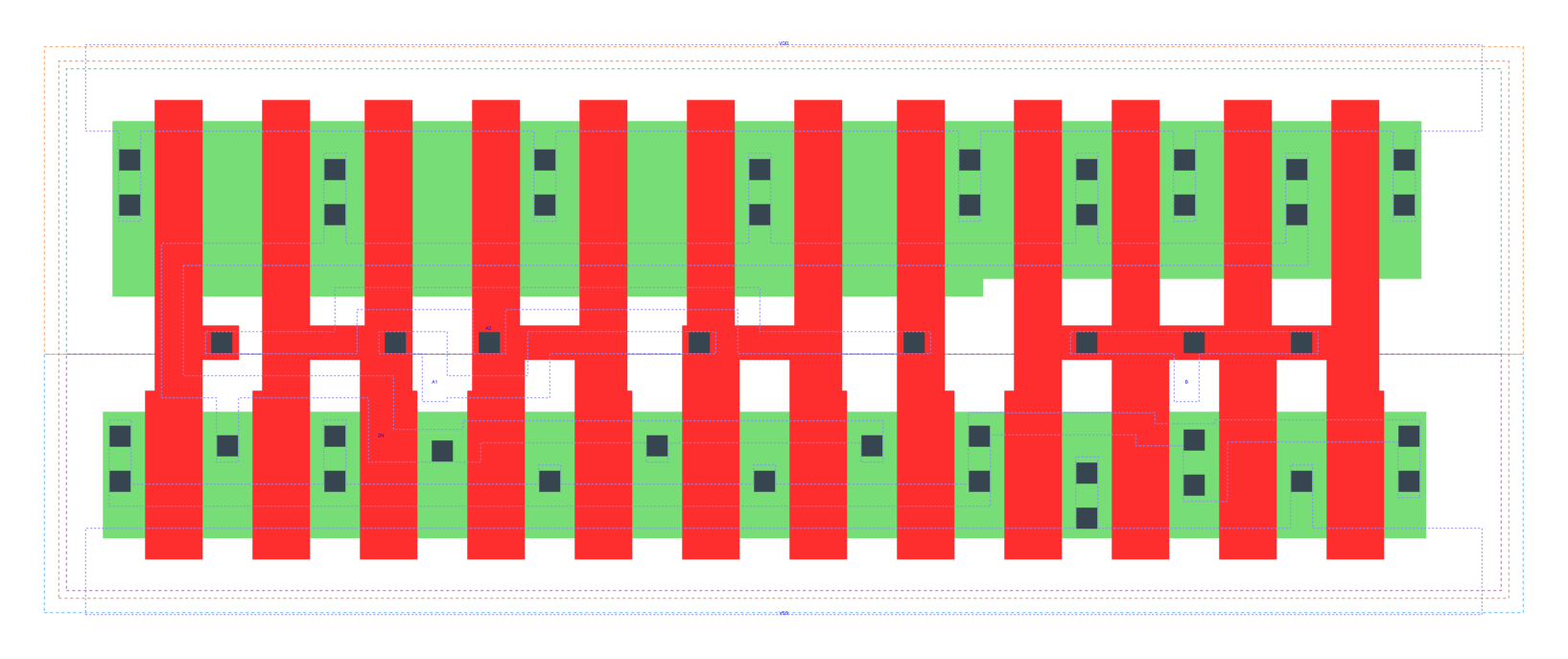
gf180mcu_fd_sc_mcu9t5v0__oai21_4 layout
Attribute |
Value |
area |
73.382400 µm2 |
Output Pin |
Function |
ZN |
(((!A1)&(!A2))|(!B)) |
A1 |
A2 |
B |
ZN |
0 |
0 |
? |
1 |
? |
? |
0 |
1 |
1 |
? |
1 |
0 |
? |
1 |
1 |
0 |
Pin |
Type |
Capacitance (pf) |
A2 |
input |
0.0280 |
A1 |
input |
0.0279 |
B |
input |
0.0255 |
Input Pin |
Output |
When Condition |
Tin (ns) |
Out Load (pf) |
Delay (ns) |
Tout (ns) |
A2(HL) |
ZN(LH) |
!A1&B |
0.0100 |
0.0010 |
0.1128 |
0.0644 |
A2(LH) |
ZN(HL) |
!A1&B |
0.0100 |
0.0010 |
0.0695 |
0.0438 |
A1(HL) |
ZN(LH) |
!A2&B |
0.0100 |
0.0010 |
0.0887 |
0.0639 |
A1(LH) |
ZN(HL) |
!A2&B |
0.0100 |
0.0010 |
0.0509 |
0.0283 |
B(LH) |
ZN(HL) |
!A1&A2 |
0.0100 |
0.0010 |
0.0916 |
0.0433 |
B(LH) |
ZN(HL) |
A1&!A2 |
0.0100 |
0.0010 |
0.0707 |
0.0287 |
B(LH) |
ZN(HL) |
A1&A2 |
0.0100 |
0.0010 |
0.0619 |
0.0287 |
B(HL) |
ZN(LH) |
!A1&A2 |
0.0100 |
0.0010 |
0.0977 |
0.0869 |
B(HL) |
ZN(LH) |
A1&!A2 |
0.0100 |
0.0010 |
0.0916 |
0.0634 |
B(HL) |
ZN(LH) |
A1&A2 |
0.0100 |
0.0010 |
0.1075 |
0.0745 |
Input Pin |
When Condition |
Tin (ns) |
Output |
Out Load (pf) |
Energy (uW/MHz) |
A1 |
!A2&B |
0.0100 |
ZN(LH) |
0.0010 |
0.6908 |
B |
!A1&A2 |
0.0100 |
ZN(HL) |
0.0010 |
0.1745 |
B |
A1&!A2 |
0.0100 |
ZN(HL) |
0.0010 |
0.0188 |
B |
A1&A2 |
0.0100 |
ZN(HL) |
0.0010 |
0.0194 |
A2 |
!A1&B |
0.0100 |
ZN(LH) |
0.0010 |
0.8693 |
A1 |
!A2&B |
0.0100 |
ZN(HL) |
0.0010 |
0.0189 |
B |
!A1&A2 |
0.0100 |
ZN(LH) |
0.0010 |
1.2788 |
B |
A1&!A2 |
0.0100 |
ZN(LH) |
0.0010 |
1.1000 |
B |
A1&A2 |
0.0100 |
ZN(LH) |
0.0010 |
1.2440 |
A2 |
!A1&B |
0.0100 |
ZN(HL) |
0.0010 |
0.1567 |
B(HL) |
!A1&!A2 |
0.0100 |
n/a |
n/a |
0.2488 |
A2(LH) |
!A1&!B |
0.0100 |
n/a |
n/a |
0.0038 |
A2(LH) |
A1&!B |
0.0100 |
n/a |
n/a |
-0.2599 |
A2(LH) |
A1&B |
0.0100 |
n/a |
n/a |
-0.1989 |
A1(LH) |
!A2&!B |
0.0100 |
n/a |
n/a |
0.0021 |
A1(LH) |
A2&!B |
0.0100 |
n/a |
n/a |
-0.2625 |
A1(LH) |
A2&B |
0.0100 |
n/a |
n/a |
-0.0674 |
A2(HL) |
!A1&!B |
0.0100 |
n/a |
n/a |
0.2675 |
A2(HL) |
A1&!B |
0.0100 |
n/a |
n/a |
0.2826 |
A2(HL) |
A1&B |
0.0100 |
n/a |
n/a |
0.2381 |
B(LH) |
!A1&!A2 |
0.0100 |
n/a |
n/a |
-0.2144 |
A1(HL) |
!A2&!B |
0.0100 |
n/a |
n/a |
0.2686 |
A1(HL) |
A2&!B |
0.0100 |
n/a |
n/a |
0.2827 |
A1(HL) |
A2&B |
0.0100 |
n/a |
n/a |
0.1624 |
When Condition |
Power (nW) |
!A1&!A2&!B |
0.2517 |
!A1&!A2&B |
0.2547 |
!A1&A2&!B |
0.4886 |
A1&!A2&!B |
0.4886 |
A1&A2&!B |
0.4898 |
!A1&A2&B |
0.4062 |
A1&!A2&B |
0.2644 |
A1&A2&B |
0.2644 |