gf180mcu_fd_sc_mcu9t5v0__xnor2_1
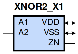
gf180mcu_fd_sc_mcu9t5v0__xnor2_1 symbol
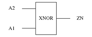
gf180mcu_fd_sc_mcu9t5v0__xnor2_1 schematic

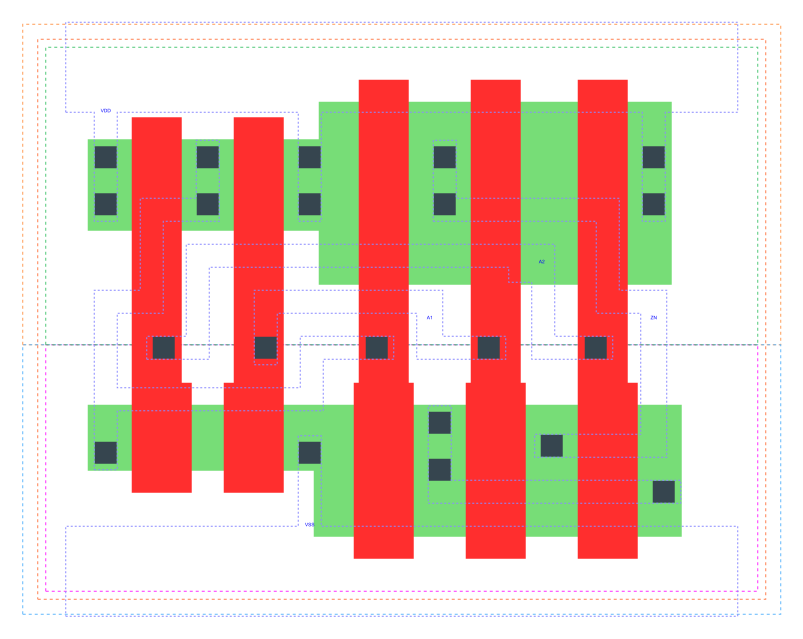
gf180mcu_fd_sc_mcu9t5v0__xnor2_1 layout
Attribute |
Value |
area |
33.868800 µm2 |
Output Pin |
Function |
ZN |
(!(A1^A2)) |
A1 |
A2 |
ZN |
1 |
1 |
1 |
0 |
0 |
1 |
1 |
0 |
0 |
0 |
1 |
0 |
Pin |
Type |
Capacitance (pf) |
A2 |
input |
0.0105 |
A1 |
input |
0.0108 |
Input Pin |
Output |
When Condition |
Tin (ns) |
Out Load (pf) |
Delay (ns) |
Tout (ns) |
A2(LH) |
ZN(LH) |
A1 |
0.0100 |
0.0010 |
0.2582 |
0.0811 |
A2(HL) |
ZN(LH) |
!A1 |
0.0100 |
0.0010 |
0.1238 |
0.0738 |
A2(HL) |
ZN(HL) |
A1 |
0.0100 |
0.0010 |
0.2158 |
0.0465 |
A2(LH) |
ZN(HL) |
!A1 |
0.0100 |
0.0010 |
0.0745 |
0.0478 |
A1(HL) |
ZN(LH) |
!A2 |
0.0100 |
0.0010 |
0.1000 |
0.0733 |
A1(HL) |
ZN(HL) |
A2 |
0.0100 |
0.0010 |
0.2573 |
0.0603 |
A1(LH) |
ZN(HL) |
!A2 |
0.0100 |
0.0010 |
0.0558 |
0.0320 |
A1(LH) |
ZN(LH) |
A2 |
0.0100 |
0.0010 |
0.2704 |
0.0812 |
Input Pin |
When Condition |
Tin (ns) |
Output |
Out Load (pf) |
Energy (uW/MHz) |
A2 |
A1 |
0.0100 |
ZN(LH) |
0.0010 |
0.2794 |
A2 |
!A1 |
0.0100 |
ZN(LH) |
0.0010 |
0.2461 |
A1 |
!A2 |
0.0100 |
ZN(LH) |
0.0010 |
0.2015 |
A1 |
A2 |
0.0100 |
ZN(LH) |
0.0010 |
0.3174 |
A1 |
A2 |
0.0100 |
ZN(HL) |
0.0010 |
0.3922 |
A1 |
!A2 |
0.0100 |
ZN(HL) |
0.0010 |
-0.0137 |
A2 |
A1 |
0.0100 |
ZN(HL) |
0.0010 |
0.3320 |
A2 |
!A1 |
0.0100 |
ZN(HL) |
0.0010 |
0.0277 |
When Condition |
Power (nW) |
!A1&!A2 |
0.1264 |
A1&A2 |
0.2131 |
!A1&A2 |
0.2046 |
A1&!A2 |
0.1292 |