gf180mcu_fd_sc_mcu9t5v0__clkinv_8
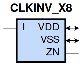
gf180mcu_fd_sc_mcu9t5v0__clkinv_8 symbol
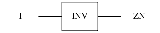
gf180mcu_fd_sc_mcu9t5v0__clkinv_8 schematic

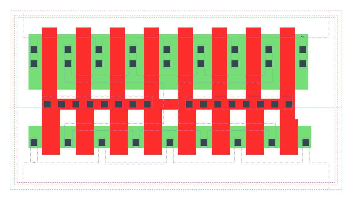
gf180mcu_fd_sc_mcu9t5v0__clkinv_8 layout
CLKINV_X8 is a clock inverter with 8X drive strength
Attributes
Attribute |
Value |
area |
50.803200 µm2 |
OUTPUT FUNCTIONS
Output Pin |
Function |
ZN |
(!I) |
TRUTH TABLE FOR ZN
I |
ZN |
0 |
1 |
1 |
0 |
FUNCTIONAL SCHEMATIC
PIN CAPACITANCE (pf)
Pin |
Type |
Capacitance (pf) |
I |
input |
0.0440 |
DELAY AND OUTPUT TRANSITION TIME corresponding to min slew and load
Input Pin |
Output |
When Condition |
Tin (ns) |
Out Load (pf) |
Delay (ns) |
Tout (ns) |
I(LH) |
ZN(HL) |
default |
0.0100 |
0.0010 |
0.0351 |
0.0133 |
I(HL) |
ZN(LH) |
default |
0.0100 |
0.0010 |
0.0265 |
0.0150 |
DYNAMIC ENERGY
Input Pin |
When Condition |
Tin (ns) |
Output |
Out Load (pf) |
Energy (uW/MHz) |
I |
default |
0.0100 |
ZN(HL) |
0.0010 |
-0.1466 |
I |
default |
0.0100 |
ZN(LH) |
0.0010 |
0.8135 |
LEAKAGE POWER
When Condition |
Power (nW) |
!I |
0.2535 |
I |
0.2649 |