gf180mcu_fd_sc_mcu9t5v0__xor2_2
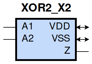
gf180mcu_fd_sc_mcu9t5v0__xor2_2 symbol
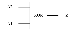
gf180mcu_fd_sc_mcu9t5v0__xor2_2 schematic

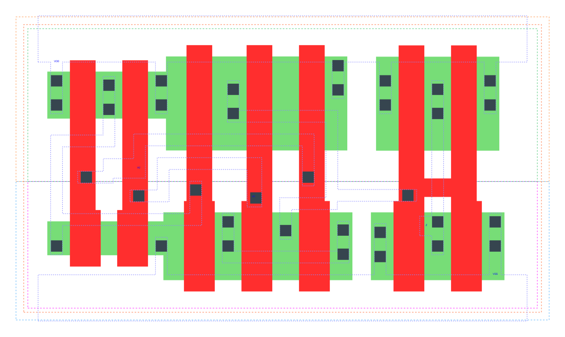
gf180mcu_fd_sc_mcu9t5v0__xor2_2 layout
Attribute |
Value |
area |
47.980800 µm2 |
Output Pin |
Function |
Z |
(A1^A2) |
A1 |
A2 |
Z |
1 |
0 |
1 |
0 |
1 |
1 |
1 |
1 |
0 |
0 |
0 |
0 |
Pin |
Type |
Capacitance (pf) |
A2 |
input |
0.0104 |
A1 |
input |
0.0108 |
Input Pin |
Output |
When Condition |
Tin (ns) |
Out Load (pf) |
Delay (ns) |
Tout (ns) |
A2(HL) |
Z(HL) |
!A1 |
0.0100 |
0.0010 |
0.2636 |
0.0394 |
A2(LH) |
Z(LH) |
!A1 |
0.0100 |
0.0010 |
0.2008 |
0.0322 |
A2(HL) |
Z(LH) |
A1 |
0.0100 |
0.0010 |
0.3426 |
0.0313 |
A2(LH) |
Z(HL) |
A1 |
0.0100 |
0.0010 |
0.3471 |
0.0328 |
A1(LH) |
Z(HL) |
A2 |
0.0100 |
0.0010 |
0.3597 |
0.0328 |
A1(HL) |
Z(LH) |
A2 |
0.0100 |
0.0010 |
0.3855 |
0.0327 |
A1(LH) |
Z(LH) |
!A2 |
0.0100 |
0.0010 |
0.1741 |
0.0305 |
A1(HL) |
Z(HL) |
!A2 |
0.0100 |
0.0010 |
0.2402 |
0.0395 |
Input Pin |
When Condition |
Tin (ns) |
Output |
Out Load (pf) |
Energy (uW/MHz) |
A2 |
!A1 |
0.0100 |
Z(HL) |
0.0010 |
0.6586 |
A2 |
A1 |
0.0100 |
Z(HL) |
0.0010 |
0.6326 |
A1 |
A2 |
0.0100 |
Z(HL) |
0.0010 |
0.6717 |
A1 |
!A2 |
0.0100 |
Z(HL) |
0.0010 |
0.6139 |
A2 |
!A1 |
0.0100 |
Z(LH) |
0.0010 |
0.3354 |
A2 |
A1 |
0.0100 |
Z(LH) |
0.0010 |
0.6282 |
A1 |
A2 |
0.0100 |
Z(LH) |
0.0010 |
0.6962 |
A1 |
!A2 |
0.0100 |
Z(LH) |
0.0010 |
0.2804 |
When Condition |
Power (nW) |
!A1&!A2 |
0.1801 |
A1&A2 |
0.2669 |
!A1&A2 |
0.2558 |
A1&!A2 |
0.1803 |