gf180mcu_fd_sc_mcu9t5v0__and2_4
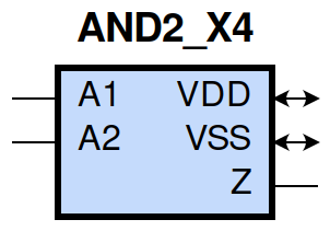
gf180mcu_fd_sc_mcu9t5v0__and2_4 symbol
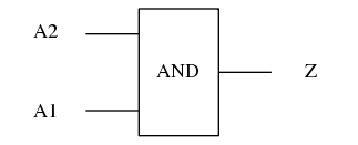
gf180mcu_fd_sc_mcu9t5v0__and2_4 schematic

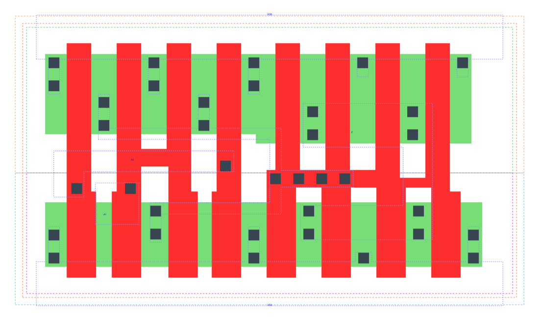
gf180mcu_fd_sc_mcu9t5v0__and2_4 layout
Attribute |
Value |
area |
47.980800 µm2 |
Output Pin |
Function |
Z |
(A1&A2) |
A1 |
A2 |
Z |
1 |
1 |
1 |
0 |
? |
0 |
? |
0 |
0 |
Pin |
Type |
Capacitance (pf) |
A2 |
input |
0.0137 |
A1 |
input |
0.0131 |
Input Pin |
Output |
When Condition |
Tin (ns) |
Out Load (pf) |
Delay (ns) |
Tout (ns) |
A2(HL) |
Z(HL) |
A1 |
0.0100 |
0.0010 |
0.1690 |
0.0284 |
A2(LH) |
Z(LH) |
A1 |
0.0100 |
0.0010 |
0.1708 |
0.0282 |
A1(LH) |
Z(LH) |
A2 |
0.0100 |
0.0010 |
0.1596 |
0.0280 |
A1(HL) |
Z(HL) |
A2 |
0.0100 |
0.0010 |
0.1512 |
0.0253 |
Input Pin |
When Condition |
Tin (ns) |
Output |
Out Load (pf) |
Energy (uW/MHz) |
A2 |
A1 |
0.0100 |
Z(HL) |
0.0010 |
1.0581 |
A2 |
A1 |
0.0100 |
Z(LH) |
0.0010 |
0.5771 |
A1 |
A2 |
0.0100 |
Z(LH) |
0.0010 |
0.5768 |
A1 |
A2 |
0.0100 |
Z(HL) |
0.0010 |
0.9121 |
A2(LH) |
!A1 |
0.0100 |
n/a |
n/a |
-0.1065 |
A1(LH) |
!A2 |
0.0100 |
n/a |
n/a |
-0.0775 |
A1(HL) |
!A2 |
0.0100 |
n/a |
n/a |
0.1214 |
A2(HL) |
!A1 |
0.0100 |
n/a |
n/a |
0.1204 |
When Condition |
Power (nW) |
!A1&!A2 |
0.2079 |
!A1&A2 |
0.2086 |
A1&!A2 |
0.2881 |
A1&A2 |
0.2593 |