gf180mcu_fd_sc_mcu9t5v0__nor2_2
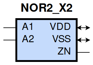
gf180mcu_fd_sc_mcu9t5v0__nor2_2 symbol
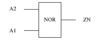
gf180mcu_fd_sc_mcu9t5v0__nor2_2 schematic

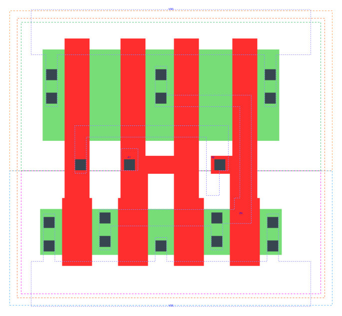
gf180mcu_fd_sc_mcu9t5v0__nor2_2 layout
Attribute |
Value |
area |
28.224000 µm2 |
Output Pin |
Function |
ZN |
((!A1)&(!A2)) |
A1 |
A2 |
ZN |
0 |
0 |
1 |
1 |
? |
0 |
? |
1 |
0 |
Pin |
Type |
Capacitance (pf) |
A2 |
input |
0.0123 |
A1 |
input |
0.0119 |
Input Pin |
Output |
When Condition |
Tin (ns) |
Out Load (pf) |
Delay (ns) |
Tout (ns) |
A2(HL) |
ZN(LH) |
!A1 |
0.0100 |
0.0010 |
0.0881 |
0.0499 |
A2(LH) |
ZN(HL) |
!A1 |
0.0100 |
0.0010 |
0.0565 |
0.0309 |
A1(HL) |
ZN(LH) |
!A2 |
0.0100 |
0.0010 |
0.0629 |
0.0483 |
A1(LH) |
ZN(HL) |
!A2 |
0.0100 |
0.0010 |
0.0397 |
0.0177 |
Input Pin |
When Condition |
Tin (ns) |
Output |
Out Load (pf) |
Energy (uW/MHz) |
A1 |
!A2 |
0.0100 |
ZN(LH) |
0.0010 |
0.2689 |
A2 |
!A1 |
0.0100 |
ZN(LH) |
0.0010 |
0.3597 |
A1 |
!A2 |
0.0100 |
ZN(HL) |
0.0010 |
-0.0281 |
A2 |
!A1 |
0.0100 |
ZN(HL) |
0.0010 |
0.0453 |
A2(LH) |
A1 |
0.0100 |
n/a |
n/a |
-0.0993 |
A1(LH) |
A2 |
0.0100 |
n/a |
n/a |
-0.0339 |
A2(HL) |
A1 |
0.0100 |
n/a |
n/a |
0.1189 |
A1(HL) |
A2 |
0.0100 |
n/a |
n/a |
0.0832 |
When Condition |
Power (nW) |
!A1&!A2 |
0.1519 |
!A1&A2 |
0.1746 |
A1&!A2 |
0.1037 |
A1&A2 |
0.1037 |