gf180mcu_fd_sc_mcu9t5v0__xor3_4
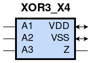
gf180mcu_fd_sc_mcu9t5v0__xor3_4 symbol
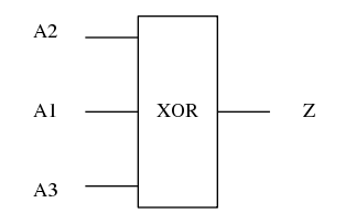
gf180mcu_fd_sc_mcu9t5v0__xor3_4 schematic

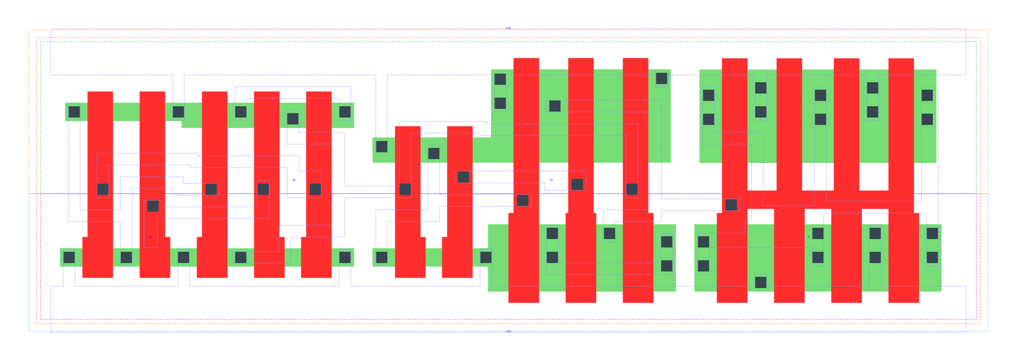
gf180mcu_fd_sc_mcu9t5v0__xor3_4 layout
Attribute |
Value |
area |
90.316800 µm2 |
Output Pin |
Function |
Z |
(A1^A2^A3) |
A1 |
A2 |
A3 |
Z |
1 |
1 |
1 |
1 |
1 |
0 |
0 |
1 |
0 |
1 |
0 |
1 |
0 |
0 |
1 |
1 |
1 |
1 |
0 |
0 |
1 |
0 |
1 |
0 |
0 |
1 |
1 |
0 |
0 |
0 |
0 |
0 |
Pin |
Type |
Capacitance (pf) |
A2 |
input |
0.0052 |
A1 |
input |
0.0052 |
A3 |
input |
0.0092 |
Input Pin |
Output |
When Condition |
Tin (ns) |
Out Load (pf) |
Delay (ns) |
Tout (ns) |
A2(HL) |
Z(HL) |
!A1&!A3 |
0.0100 |
0.0010 |
0.9605 |
0.0623 |
A2(HL) |
Z(HL) |
A1&A3 |
0.0100 |
0.0010 |
1.1162 |
0.0476 |
A2(LH) |
Z(LH) |
!A1&!A3 |
0.0100 |
0.0010 |
1.0213 |
0.0515 |
A2(LH) |
Z(LH) |
A1&A3 |
0.0100 |
0.0010 |
0.8067 |
0.0447 |
A2(HL) |
Z(LH) |
!A1&A3 |
0.0100 |
0.0010 |
1.1089 |
0.0449 |
A2(HL) |
Z(LH) |
A1&!A3 |
0.0100 |
0.0010 |
0.9230 |
0.0522 |
A2(LH) |
Z(HL) |
!A1&A3 |
0.0100 |
0.0010 |
1.2164 |
0.0474 |
A2(LH) |
Z(HL) |
A1&!A3 |
0.0100 |
0.0010 |
0.6566 |
0.0630 |
A1(LH) |
Z(HL) |
!A2&A3 |
0.0100 |
0.0010 |
1.2611 |
0.0474 |
A1(LH) |
Z(HL) |
A2&!A3 |
0.0100 |
0.0010 |
0.6454 |
0.0629 |
A1(HL) |
Z(LH) |
!A2&A3 |
0.0100 |
0.0010 |
1.1378 |
0.0445 |
A1(HL) |
Z(LH) |
A2&!A3 |
0.0100 |
0.0010 |
0.8841 |
0.0515 |
A1(LH) |
Z(LH) |
!A2&!A3 |
0.0100 |
0.0010 |
1.0679 |
0.0523 |
A1(LH) |
Z(LH) |
A2&A3 |
0.0100 |
0.0010 |
0.7955 |
0.0447 |
A1(HL) |
Z(HL) |
!A2&!A3 |
0.0100 |
0.0010 |
0.9891 |
0.0623 |
A1(HL) |
Z(HL) |
A2&A3 |
0.0100 |
0.0010 |
1.0793 |
0.0476 |
A3(LH) |
Z(LH) |
!A1&!A2 |
0.0100 |
0.0010 |
0.2568 |
0.0434 |
A3(LH) |
Z(LH) |
A1&A2 |
0.0100 |
0.0010 |
0.2570 |
0.0435 |
A3(HL) |
Z(LH) |
!A1&A2 |
0.0100 |
0.0010 |
0.5579 |
0.0466 |
A3(HL) |
Z(LH) |
A1&!A2 |
0.0100 |
0.0010 |
0.5579 |
0.0466 |
A3(HL) |
Z(HL) |
!A1&!A2 |
0.0100 |
0.0010 |
0.3600 |
0.0618 |
A3(HL) |
Z(HL) |
A1&A2 |
0.0100 |
0.0010 |
0.3596 |
0.0618 |
A3(LH) |
Z(HL) |
!A1&A2 |
0.0100 |
0.0010 |
0.4980 |
0.0475 |
A3(LH) |
Z(HL) |
A1&!A2 |
0.0100 |
0.0010 |
0.4980 |
0.0475 |
Input Pin |
When Condition |
Tin (ns) |
Output |
Out Load (pf) |
Energy (uW/MHz) |
A3 |
!A1&!A2 |
0.0100 |
Z(LH) |
0.0010 |
0.7662 |
A3 |
A1&A2 |
0.0100 |
Z(LH) |
0.0010 |
0.7670 |
A3 |
!A1&A2 |
0.0100 |
Z(LH) |
0.0010 |
1.2171 |
A3 |
A1&!A2 |
0.0100 |
Z(LH) |
0.0010 |
1.2171 |
A2 |
!A1&!A3 |
0.0100 |
Z(HL) |
0.0010 |
1.5659 |
A2 |
A1&A3 |
0.0100 |
Z(HL) |
0.0010 |
1.5255 |
A2 |
!A1&A3 |
0.0100 |
Z(HL) |
0.0010 |
1.5143 |
A2 |
A1&!A3 |
0.0100 |
Z(HL) |
0.0010 |
1.4077 |
A1 |
!A2&A3 |
0.0100 |
Z(HL) |
0.0010 |
1.5448 |
A1 |
A2&!A3 |
0.0100 |
Z(HL) |
0.0010 |
1.4008 |
A1 |
!A2&!A3 |
0.0100 |
Z(HL) |
0.0010 |
1.5760 |
A1 |
A2&A3 |
0.0100 |
Z(HL) |
0.0010 |
1.5046 |
A2 |
!A1&!A3 |
0.0100 |
Z(LH) |
0.0010 |
1.4182 |
A2 |
A1&A3 |
0.0100 |
Z(LH) |
0.0010 |
1.1123 |
A2 |
!A1&A3 |
0.0100 |
Z(LH) |
0.0010 |
1.2820 |
A2 |
A1&!A3 |
0.0100 |
Z(LH) |
0.0010 |
1.4510 |
A1 |
!A2&A3 |
0.0100 |
Z(LH) |
0.0010 |
1.2929 |
A1 |
A2&!A3 |
0.0100 |
Z(LH) |
0.0010 |
1.4077 |
A1 |
!A2&!A3 |
0.0100 |
Z(LH) |
0.0010 |
1.4703 |
A1 |
A2&A3 |
0.0100 |
Z(LH) |
0.0010 |
1.1055 |
A3 |
!A1&!A2 |
0.0100 |
Z(HL) |
0.0010 |
1.3278 |
A3 |
A1&A2 |
0.0100 |
Z(HL) |
0.0010 |
1.3277 |
A3 |
!A1&A2 |
0.0100 |
Z(HL) |
0.0010 |
1.2032 |
A3 |
A1&!A2 |
0.0100 |
Z(HL) |
0.0010 |
1.2032 |
When Condition |
Power (nW) |
!A1&!A2&!A3 |
0.3948 |
!A1&A2&A3 |
0.4011 |
A1&!A2&A3 |
0.4776 |
A1&A2&!A3 |
0.3122 |
!A1&!A2&A3 |
0.3942 |
!A1&A2&!A3 |
0.3904 |
A1&!A2&!A3 |
0.4669 |
A1&A2&A3 |
0.3117 |