gf180mcu_fd_sc_mcu9t5v0__nand2_1
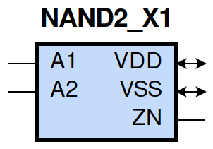
gf180mcu_fd_sc_mcu9t5v0__nand2_1 symbol
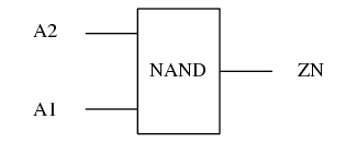
gf180mcu_fd_sc_mcu9t5v0__nand2_1 schematic

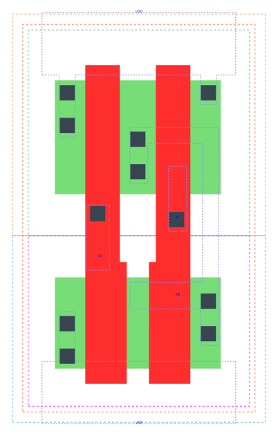
gf180mcu_fd_sc_mcu9t5v0__nand2_1 layout
Attribute |
Value |
area |
14.112000 µm2 |
Output Pin |
Function |
ZN |
((!A1)|(!A2)) |
A1 |
A2 |
ZN |
0 |
? |
1 |
? |
0 |
1 |
1 |
1 |
0 |
Pin |
Type |
Capacitance (pf) |
A2 |
input |
0.0065 |
A1 |
input |
0.0066 |
Input Pin |
Output |
When Condition |
Tin (ns) |
Out Load (pf) |
Delay (ns) |
Tout (ns) |
A2(HL) |
ZN(LH) |
A1 |
0.0100 |
0.0010 |
0.0767 |
0.0527 |
A2(LH) |
ZN(HL) |
A1 |
0.0100 |
0.0010 |
0.0613 |
0.0279 |
A1(HL) |
ZN(LH) |
A2 |
0.0100 |
0.0010 |
0.0567 |
0.0350 |
A1(LH) |
ZN(HL) |
A2 |
0.0100 |
0.0010 |
0.0499 |
0.0280 |
Input Pin |
When Condition |
Tin (ns) |
Output |
Out Load (pf) |
Energy (uW/MHz) |
A1 |
A2 |
0.0100 |
ZN(LH) |
0.0010 |
0.1526 |
A2 |
A1 |
0.0100 |
ZN(LH) |
0.0010 |
0.2117 |
A1 |
A2 |
0.0100 |
ZN(HL) |
0.0010 |
0.0012 |
A2 |
A1 |
0.0100 |
ZN(HL) |
0.0010 |
0.0011 |
A2(LH) |
!A1 |
0.0100 |
n/a |
n/a |
-0.0539 |
A1(LH) |
!A2 |
0.0100 |
n/a |
n/a |
-0.0386 |
A2(HL) |
!A1 |
0.0100 |
n/a |
n/a |
0.0605 |
A1(HL) |
!A2 |
0.0100 |
n/a |
n/a |
0.0616 |
When Condition |
Power (nW) |
!A1&!A2 |
0.0753 |
!A1&A2 |
0.0756 |
A1&!A2 |
0.1154 |
A1&A2 |
0.1035 |