gf180mcu_fd_sc_mcu9t5v0__or2_4
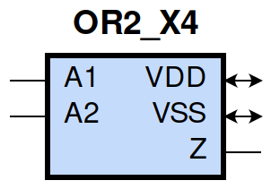
gf180mcu_fd_sc_mcu9t5v0__or2_4 symbol
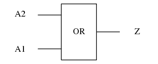
gf180mcu_fd_sc_mcu9t5v0__or2_4 schematic

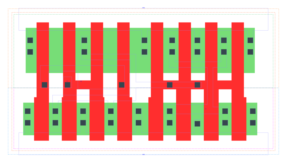
gf180mcu_fd_sc_mcu9t5v0__or2_4 layout
Attribute |
Value |
area |
50.803200 µm2 |
Output Pin |
Function |
Z |
(A1|A2) |
A1 |
A2 |
Z |
1 |
? |
1 |
? |
1 |
1 |
0 |
0 |
0 |
Pin |
Type |
Capacitance (pf) |
A2 |
input |
0.0141 |
A1 |
input |
0.0136 |
Input Pin |
Output |
When Condition |
Tin (ns) |
Out Load (pf) |
Delay (ns) |
Tout (ns) |
A2(HL) |
Z(HL) |
!A1 |
0.0100 |
0.0010 |
0.2448 |
0.0369 |
A2(LH) |
Z(LH) |
!A1 |
0.0100 |
0.0010 |
0.1370 |
0.0239 |
A1(LH) |
Z(LH) |
!A2 |
0.0100 |
0.0010 |
0.1204 |
0.0229 |
A1(HL) |
Z(HL) |
!A2 |
0.0100 |
0.0010 |
0.2206 |
0.0368 |
Input Pin |
When Condition |
Tin (ns) |
Output |
Out Load (pf) |
Energy (uW/MHz) |
A2 |
!A1 |
0.0100 |
Z(HL) |
0.0010 |
1.2077 |
A2 |
!A1 |
0.0100 |
Z(LH) |
0.0010 |
0.5699 |
A1 |
!A2 |
0.0100 |
Z(LH) |
0.0010 |
0.4879 |
A1 |
!A2 |
0.0100 |
Z(HL) |
0.0010 |
1.1174 |
A2(LH) |
A1 |
0.0100 |
n/a |
n/a |
-0.0992 |
A1(LH) |
A2 |
0.0100 |
n/a |
n/a |
-0.0334 |
A1(HL) |
A2 |
0.0100 |
n/a |
n/a |
0.0790 |
A2(HL) |
A1 |
0.0100 |
n/a |
n/a |
0.1187 |
When Condition |
Power (nW) |
!A1&!A2 |
0.2598 |
!A1&A2 |
0.2770 |
A1&!A2 |
0.2060 |
A1&A2 |
0.2060 |