gf180mcu_fd_sc_mcu9t5v0__nand2_4
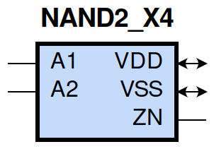
gf180mcu_fd_sc_mcu9t5v0__nand2_4 symbol
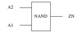
gf180mcu_fd_sc_mcu9t5v0__nand2_4 schematic

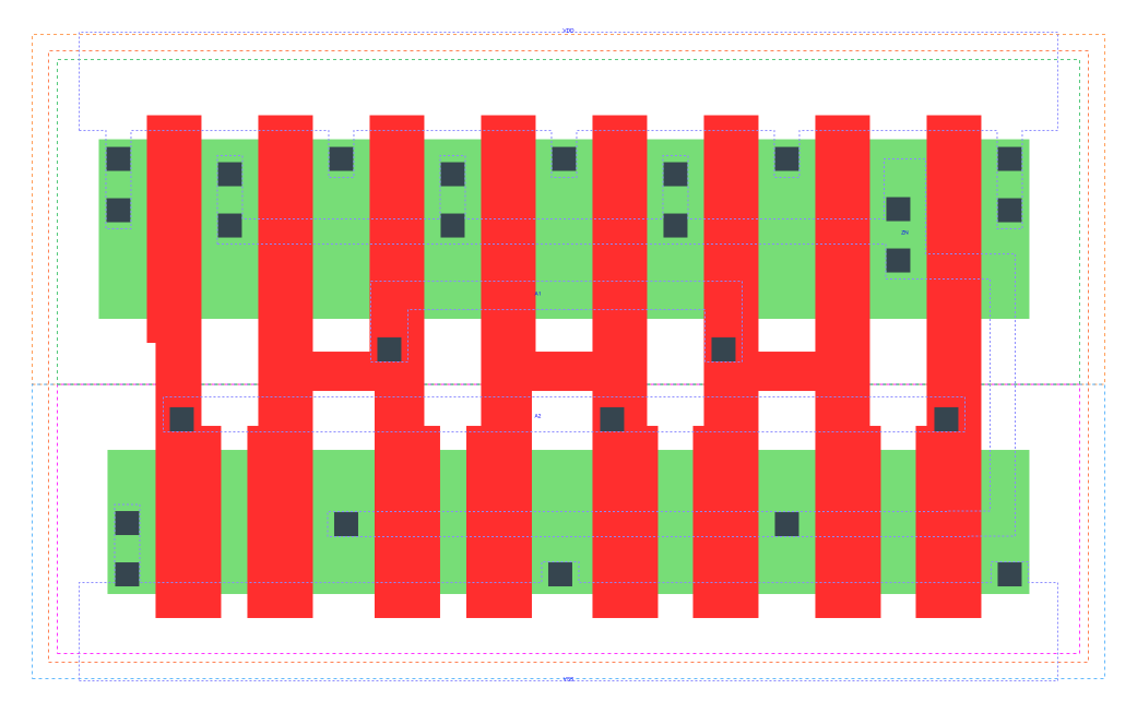
gf180mcu_fd_sc_mcu9t5v0__nand2_4 layout
Attribute |
Value |
area |
45.158400 µm2 |
Output Pin |
Function |
ZN |
((!A1)|(!A2)) |
A1 |
A2 |
ZN |
0 |
? |
1 |
? |
0 |
1 |
1 |
1 |
0 |
Pin |
Type |
Capacitance (pf) |
A2 |
input |
0.0263 |
A1 |
input |
0.0259 |
Input Pin |
Output |
When Condition |
Tin (ns) |
Out Load (pf) |
Delay (ns) |
Tout (ns) |
A2(HL) |
ZN(LH) |
A1 |
0.0100 |
0.0010 |
0.0661 |
0.0439 |
A2(LH) |
ZN(HL) |
A1 |
0.0100 |
0.0010 |
0.0532 |
0.0213 |
A1(HL) |
ZN(LH) |
A2 |
0.0100 |
0.0010 |
0.0459 |
0.0265 |
A1(LH) |
ZN(HL) |
A2 |
0.0100 |
0.0010 |
0.0421 |
0.0212 |
Input Pin |
When Condition |
Tin (ns) |
Output |
Out Load (pf) |
Energy (uW/MHz) |
A1 |
A2 |
0.0100 |
ZN(LH) |
0.0010 |
0.5361 |
A2 |
A1 |
0.0100 |
ZN(LH) |
0.0010 |
0.7759 |
A1 |
A2 |
0.0100 |
ZN(HL) |
0.0010 |
0.0013 |
A2 |
A1 |
0.0100 |
ZN(HL) |
0.0010 |
0.0011 |
A2(LH) |
!A1 |
0.0100 |
n/a |
n/a |
-0.2145 |
A1(LH) |
!A2 |
0.0100 |
n/a |
n/a |
-0.1574 |
A2(HL) |
!A1 |
0.0100 |
n/a |
n/a |
0.2417 |
A1(HL) |
!A2 |
0.0100 |
n/a |
n/a |
0.2450 |
When Condition |
Power (nW) |
!A1&!A2 |
0.1510 |
!A1&A2 |
0.1523 |
A1&!A2 |
0.3114 |
A1&A2 |
0.2640 |