gf180mcu_fd_sc_mcu9t5v0__oai21_2
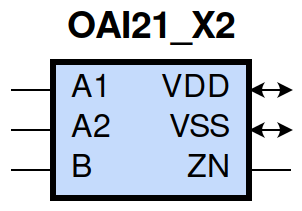
gf180mcu_fd_sc_mcu9t5v0__oai21_2 symbol
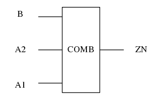
gf180mcu_fd_sc_mcu9t5v0__oai21_2 schematic

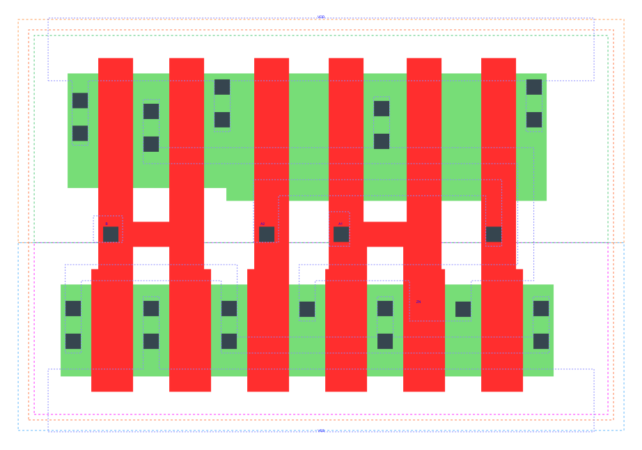
gf180mcu_fd_sc_mcu9t5v0__oai21_2 layout
Attribute |
Value |
area |
39.513600 µm2 |
Output Pin |
Function |
ZN |
(((!A1)&(!A2))|(!B)) |
A1 |
A2 |
B |
ZN |
0 |
0 |
? |
1 |
? |
? |
0 |
1 |
1 |
? |
1 |
0 |
? |
1 |
1 |
0 |
Pin |
Type |
Capacitance (pf) |
B |
input |
0.0127 |
A2 |
input |
0.0139 |
A1 |
input |
0.0135 |
Input Pin |
Output |
When Condition |
Tin (ns) |
Out Load (pf) |
Delay (ns) |
Tout (ns) |
B(LH) |
ZN(HL) |
!A1&A2 |
0.0100 |
0.0010 |
0.0942 |
0.0443 |
B(LH) |
ZN(HL) |
A1&!A2 |
0.0100 |
0.0010 |
0.0733 |
0.0301 |
B(LH) |
ZN(HL) |
A1&A2 |
0.0100 |
0.0010 |
0.0641 |
0.0298 |
B(HL) |
ZN(LH) |
!A1&A2 |
0.0100 |
0.0010 |
0.1015 |
0.0900 |
B(HL) |
ZN(LH) |
A1&!A2 |
0.0100 |
0.0010 |
0.0955 |
0.0667 |
B(HL) |
ZN(LH) |
A1&A2 |
0.0100 |
0.0010 |
0.1116 |
0.0779 |
A2(HL) |
ZN(LH) |
!A1&B |
0.0100 |
0.0010 |
0.1154 |
0.0669 |
A2(LH) |
ZN(HL) |
!A1&B |
0.0100 |
0.0010 |
0.0705 |
0.0448 |
A1(HL) |
ZN(LH) |
!A2&B |
0.0100 |
0.0010 |
0.0918 |
0.0664 |
A1(LH) |
ZN(HL) |
!A2&B |
0.0100 |
0.0010 |
0.0521 |
0.0295 |
Input Pin |
When Condition |
Tin (ns) |
Output |
Out Load (pf) |
Energy (uW/MHz) |
A1 |
!A2&B |
0.0100 |
ZN(LH) |
0.0010 |
0.3472 |
B |
!A1&A2 |
0.0100 |
ZN(HL) |
0.0010 |
0.0848 |
B |
A1&!A2 |
0.0100 |
ZN(HL) |
0.0010 |
0.0090 |
B |
A1&A2 |
0.0100 |
ZN(HL) |
0.0010 |
0.0093 |
A2 |
!A1&B |
0.0100 |
ZN(LH) |
0.0010 |
0.4357 |
A1 |
!A2&B |
0.0100 |
ZN(HL) |
0.0010 |
0.0092 |
B |
!A1&A2 |
0.0100 |
ZN(LH) |
0.0010 |
0.6530 |
B |
A1&!A2 |
0.0100 |
ZN(LH) |
0.0010 |
0.5643 |
B |
A1&A2 |
0.0100 |
ZN(LH) |
0.0010 |
0.6367 |
A2 |
!A1&B |
0.0100 |
ZN(HL) |
0.0010 |
0.0758 |
B(HL) |
!A1&!A2 |
0.0100 |
n/a |
n/a |
0.1242 |
A2(LH) |
!A1&!B |
0.0100 |
n/a |
n/a |
0.0147 |
A2(LH) |
A1&!B |
0.0100 |
n/a |
n/a |
-0.1299 |
A2(LH) |
A1&B |
0.0100 |
n/a |
n/a |
-0.0995 |
A1(LH) |
!A2&!B |
0.0100 |
n/a |
n/a |
0.0136 |
A1(LH) |
A2&!B |
0.0100 |
n/a |
n/a |
-0.1315 |
A1(LH) |
A2&B |
0.0100 |
n/a |
n/a |
-0.0338 |
A2(HL) |
!A1&!B |
0.0100 |
n/a |
n/a |
0.1340 |
A2(HL) |
A1&!B |
0.0100 |
n/a |
n/a |
0.1406 |
A2(HL) |
A1&B |
0.0100 |
n/a |
n/a |
0.1189 |
B(LH) |
!A1&!A2 |
0.0100 |
n/a |
n/a |
-0.1073 |
A1(HL) |
!A2&!B |
0.0100 |
n/a |
n/a |
0.1344 |
A1(HL) |
A2&!B |
0.0100 |
n/a |
n/a |
0.1406 |
A1(HL) |
A2&B |
0.0100 |
n/a |
n/a |
0.0794 |
When Condition |
Power (nW) |
!A1&!A2&!B |
0.1509 |
!A1&!A2&B |
0.1523 |
!A1&A2&!B |
0.2703 |
A1&!A2&!B |
0.2703 |
A1&A2&!B |
0.2709 |
!A1&A2&B |
0.2281 |
A1&!A2&B |
0.1572 |
A1&A2&B |
0.1572 |