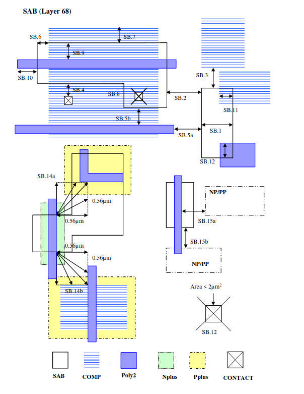
7.10 Salicide Block (SAB)
RULE NO. |
DESCRIPTION |
LAYOUT RULE |
Layer |
SB = Salicide Block |
|
SB.1 |
Width |
0.42 |
SB.2 |
Space |
0.42 |
SB.3 |
Space from salicide block to unrelated COMP |
0.22 |
SB.4 |
Space from salicide block to contact |
0.15 |
SB.5a |
Space from salicide block to unrelated Poly2 on field |
0.3 |
SB.5b |
Space from salicide block to unrelated Poly2 on COMP |
0.28 |
SB.6 |
Salicide block extension beyond related COMP |
0.22 |
SB.7 |
COMP extension beyond related salicide block |
0.22 |
SB.8 |
Non-salicided contacts are forbidden |
|
SB.9 |
Salicide block extension beyond unsalicided Poly2 |
0.22 |
SB.10 |
Poly2 extension beyond related salicide block |
0.22 |
SB.11 |
Overlap with COMP |
0.22 |
SB.12 |
Overlap with Poly2 outside ESD_MK |
0.22 |
SB.13 |
Min. area |
2.0 μm2 |
SB.14a |
Space from unsalicided Nplus Poly2 to unsalicided Pplus Poly2 (Unsalicided Nplus Poly2 must not fall within a square of 0.56μm x 0.56μm at unsalicided Pplus Poly2 corners) |
0.56 |
SB.14b |
Space from unsalicided Nplus Poly2 to P-channel gate (Unsalicided Nplus Poly2 must not fall within a square of 0.56μm x 0.56μm at P-channel gate corners) |
0.56 |
SB.15a |
Space from unsalicided Poly2 to unrelated Nplus/Pplus |
0.18 |
SB.15b |
Space from unsalicided Poly2 to unrelated Nplus/Pplus along Poly2 line |
0.32 |
SB.16 |
SAB layer cannot exist on 3.3V and 5V/6V CMOS transistors’ Poly and COMP area of the core circuit (Excluding the transistors used for ESD purpose). It can only exist on CMOS transistors marked by LVS_IO, OTP_MK, ESD_MK layers. |