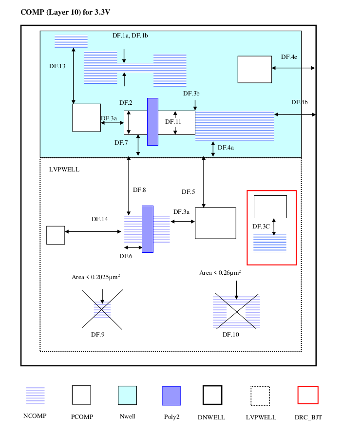
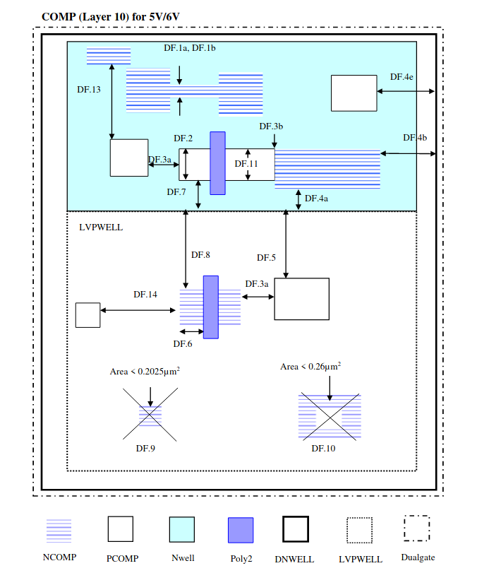
7.5 Comp
These rules apply for COMP inside as well as outside DNWELL unless stated specifically.
RULE NO. |
DESCRIPTION |
LAYOUT RULE |
|
Layer |
DF = Diffusion / Active / Composite |
3.3V |
5V/6V |
DF.1a |
Min. COMP Width |
0.22 |
0.3 |
DF.1b* |
Min. COMP Width as a resistor with low sheet resistivity |
0.3 |
0.3 |
DF.1c |
Min. COMP Width for MOSCAP |
1 |
1 |
DF.2a |
Min Channel Width |
0.22 |
0.3 |
DF.2b |
Max. COMP width for all cases except those used for capacitors, marked by “MOS_CAP_MK” layer. |
100 |
100 |
DF.3a |
Min. COMP Space. P-substrate tap (PCOMP outside NWELL and DNWELL) can be butted for different voltage devices as the potential is same |
0.28 |
0.36 |
DF.3b |
Min./Max. NCOMP Space to PCOMP in the same well for butted COMP (MOSCAP butting is not allowed) |
0 |
0 |
DF.3c |
Min. COMP Space in BJT area (area marked by DRC_BJT layer) |
0.32 |
NA |
DF.4a |
Min. (LVPWELL Space to NCOMP well tap) inside DNWELL |
0.12 |
0.16 |
DF.4b |
Min. DNWELL overlap of NCOMP well tap |
0.62 |
0.66 |
DF.4c |
Min. (Nwell overlap of PCOMP) outside DNWELL |
0.43 |
0.6 |
DF.4d |
Min. (Nwell overlap of NCOMP) outside DNWELL |
0.12 |
0.16 |
DF.4e |
Min. DNWELL overlap of PCOMP |
0.93 |
1.1 |
DF.5 |
Min. (LVPWELL overlap of PCOMP well tap) inside DNWELL |
0.12 |
0.16 |
DF.6 |
Min. COMP extend beyond gate (it also means source/drain overhang) |
0.24 |
0.4 |
DF.7 |
Min. (LVPWELL Spacer to PCOMP) inside DNWELL. |
0.43 |
0.6 |
DF.8 |
Min. (LVPWELL overlap of NCOMP) Inside DNWELL |
0.43 |
0.6 |
DF.9 |
Min. COMP area (um2) |
0.2025 |
0.2025 |
DF.10 |
Min. field area (um2) |
0.26 |
0.26 |
DF.11 |
Min. Length of butting COMP edge |
0.3 |
0.3 |
DF.12 |
COMP not covered by Nplus or Pplus is forbidden (except those COMP under marking). |
||
DF.13 |
Max distance of Nwell tap (NCOMP inside Nwell) from (PCOMP inside Nwell) |
20 |
15 |
DF.14 |
Max distance of substrate tap (PCOMP outside Nwell) from (NCOMP outside Nwell) |
20 |
15 |
DF.15a** |
NCOMP inside DNWELL and Dualgate, but outside LVPWELL i.e. [(NCOMP AND DNWELL AND Dualgate) AND (NOT LVPWELL)] can only be connected to 5V/6V VDD.” |
||
DF.15b** |
NCOMP inside DNWELL but outside Dualgate and LVPWELL i.e.[(NCOMP AND DNWELL) AND (NOT Dualgate) AND ( NOT LVPWELL) can only be connected to 3.3V VDD. |
Rules specific to 3.3V/(5V)6V COMP outside DNWELL
RULE NO. |
DESCRIPTION |
LAYOUT RULE |
|
Layer |
DF = Diffusion / Active / Composite |
3.3V |
5V/6V |
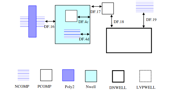
DF.16 |
Min. space from (Nwell outside DNWELL) to (NCOMP outside Nwell and DNWELL). |
0.43 |
0.6 |
DF.17 |
Min. space from (Nwell Outside DNWELL) to (PCOMP outside Nwell and DNWELL) |
0.12 |
0.16 |
DF.18 |
Min. DNWELL space to (PCOMP outside Nwell and DNWELL) |
2.5 |
2.5 |
DF.19 |
Min. DNWELL space to (NCOMP outside Nwell and DNWELL) |
3.2 |
3.28 |
Note
** This rule can be detected by ERC, not by DRC
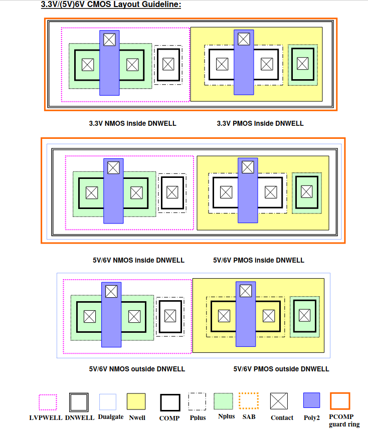
3.3V/(5V)6V CMOS Layout Guideline: